- 您現(xiàn)在的位置:買賣IC網(wǎng) > PDF目錄368672 > TMS320UVC5409 16-Bit Digital Signal Processor PDF資料下載
參數(shù)資料
| 型號: | TMS320UVC5409 |
| 元件分類: | 數(shù)字信號處理 |
| 英文描述: | 16-Bit Digital Signal Processor |
| 中文描述: | 16位數(shù)字信號處理器 |
| 文件頁數(shù): | 51/60頁 |
| 文件大?。?/td> | 772K |
| 代理商: | TMS320UVC5409 |
第1頁第2頁第3頁第4頁第5頁第6頁第7頁第8頁第9頁第10頁第11頁第12頁第13頁第14頁第15頁第16頁第17頁第18頁第19頁第20頁第21頁第22頁第23頁第24頁第25頁第26頁第27頁第28頁第29頁第30頁第31頁第32頁第33頁第34頁第35頁第36頁第37頁第38頁第39頁第40頁第41頁第42頁第43頁第44頁第45頁第46頁第47頁第48頁第49頁第50頁當(dāng)前第51頁第52頁第53頁第54頁第55頁第56頁第57頁第58頁第59頁第60頁
TMS320UVC5402
FIXED-POINT DIGITAL SIGNAL PROCESSOR
SPRS100A – APRIL 1999 – REVISED AUGUST 1999
51
POST OFFICE BOX 1443
HOUSTON, TEXAS 77251–1443
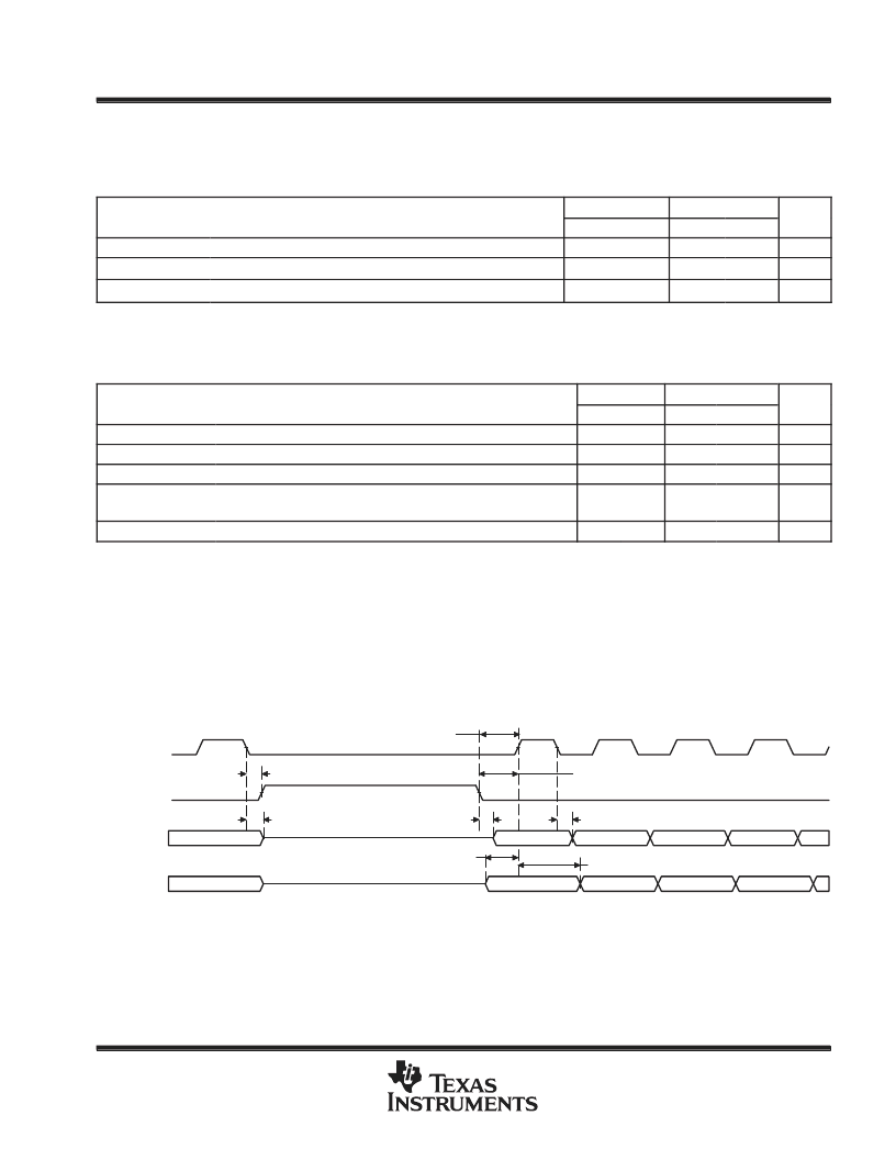
multichannel buffered serial port timing (continued)
timing requirements for McBSP as SPI master or slave: [H=0.5t
c(CO)
] CLKSTP = 11b, CLKXP = 0
(see Figure 28)
MASTER
SLAVE
UNIT
MIN
MAX
MIN
MAX
tsu(BDRV-BCKXH)
th(BCKXH-BDRV)
tsu(BFXL-BCKXH)
For all SPI slave modes, CLKG is programmed as 1/2 of the CPU clock by setting CLKSM = CLKGDV = 1.
Setup time, BDR valid before BCLKX high
15
–12H
ns
Hold time, BDR valid after BCLKX high
6
5+12H
ns
Setup time, BFSX low before BCLKX high
15
ns
switching characteristics for McBSP as SPI master or slave: [H=0.5t
c(CO)
] CLKSTP = 11b,
CLKXP = 0
(see Figure 28)
PARAMETER
MASTER
SLAVE
UNIT
MIN
MAX
MIN
MAX
th(BCKXL-BFXL)
td(BFXL-BCKXH)
td(BCKXL-BDXV)
Hold time, BFSX low after BCLKX low§
Delay time, BFSX low to BCLKX high
C–2
C+3
ns
T–2
T+3
ns
Delay time, BCLKX low to BDX valid
0
6
6H+10
10H+25
ns
tdis(BCKXL-BDXHZ)
Disable time, BDX high impedance following last data bit from
BCLKX low
0
6
6H+10
10H+25
ns
td(BFXL-BDXV)
For all SPI slave modes, CLKG is programmed as 1/2 of the CPU clock by setting CLKSM = CLKGDV = 1.
T =
BCLKX period = (1 + CLKGDV) * 2H
C =
BCLKX low pulse width = T/2 when CLKGDV is odd or zero and = (CLKGDV/2) * 2H when CLKGDV is even
D =
BCLKX high pulse width = T/2 when CLKGDV is odd or zero and = (CLKGDV/2 + 1) * 2H when CLKGDV is even
§FSRP = FSXP = 1. As a SPI master, BFSX is inverted to provide active-low slave-enable output. As a slave, the active-low signal input on BFSX
and BFSR is inverted before being used internally.
CLKXM = FSXM = 1, CLKRM = FSRM = 0 for master McBSP
CLKXM = CLKRM = FSXM = FSRM = 0 for slave McBSP
BFSX should be low before the rising edge of clock to enable slave devices and then begin a SPI transfer at the rising edge of the master clock
(BCLKX).
Delay time, BFSX low to BDX valid
D–2
D+4
4H+10
8H+25
ns
Bit 0
Bit(n-1)
(n-2)
(n-3)
(n-4)
Bit 0
Bit(n-1)
(n-2)
(n-3)
(n-4)
BCLKX
BFSX
BDX
BDR
td(BFXL-BCKXH)
tdis(BCKXL-BDXHZ)
td(BCKXL-BDXV)
th(BCKXH-BDRV)
tsu(BDRV-BCKXH)
td(BFXL-BDXV)
th(BCKXL-BFXL)
LSB
MSB
tsu(BFXL-BCKXH)
Figure 28. McBSP Timing as SPI Master or Slave: CLKSTP = 11b, CLKXP = 0
P
相關(guān)PDF資料 |
PDF描述 |
|---|---|
| TMS320UVC5402 | Fixed-Point Digital Signal Processor(定點DSP) |
| TMS320VC5409PGE-100 | 16-Bit Digital Signal Processor |
| TMS320VC5409GGU-100 | 16-Bit Digital Signal Processor |
| TMS370C736AFNT | 8-BIT MICROCONTROLLER |
| SE370C758BFZT | 8-BIT MICROCONTROLLER |
相關(guān)代理商/技術(shù)參數(shù) |
參數(shù)描述 |
|---|---|
| TMS320V34PJ | 制造商:Texas Instruments 功能描述: |
| TMS320V34PJX2 | 制造商:Rochester Electronics LLC 功能描述:- Bulk 制造商:Texas Instruments 功能描述: |
| TMS320V640AGDK4 | 制造商:Texas Instruments 功能描述:TMS320DM640 548PIN FCBGA PG2.0 400 MHZ - Trays |
| TMS320V640AGNZ4 | 制造商:Texas Instruments 功能描述:TMS320DM640 548PIN FCBGA PG2.0 - Trays |
| TMS320V641AGDK5 | 制造商:Texas Instruments 功能描述:TMS320DM641AGDK PG2 548 PIN FCBGA 500MHZ - Trays |
發(fā)布緊急采購,3分鐘左右您將得到回復(fù)。