- 您現(xiàn)在的位置:買賣IC網(wǎng) > PDF目錄378055 > PM73121 (PMC-SIERRA INC) AAL1 Segmentation And Reassembly Processor PDF資料下載
參數(shù)資料
| 型號(hào): | PM73121 |
| 廠商: | PMC-SIERRA INC |
| 元件分類: | 數(shù)字傳輸電路 |
| 英文描述: | AAL1 Segmentation And Reassembly Processor |
| 中文描述: | ATM SEGMENTATION AND REASSEMBLY DEVICE |
| 文件頁數(shù): | 120/223頁 |
| 文件大小: | 2300K |
| 代理商: | PM73121 |
第1頁第2頁第3頁第4頁第5頁第6頁第7頁第8頁第9頁第10頁第11頁第12頁第13頁第14頁第15頁第16頁第17頁第18頁第19頁第20頁第21頁第22頁第23頁第24頁第25頁第26頁第27頁第28頁第29頁第30頁第31頁第32頁第33頁第34頁第35頁第36頁第37頁第38頁第39頁第40頁第41頁第42頁第43頁第44頁第45頁第46頁第47頁第48頁第49頁第50頁第51頁第52頁第53頁第54頁第55頁第56頁第57頁第58頁第59頁第60頁第61頁第62頁第63頁第64頁第65頁第66頁第67頁第68頁第69頁第70頁第71頁第72頁第73頁第74頁第75頁第76頁第77頁第78頁第79頁第80頁第81頁第82頁第83頁第84頁第85頁第86頁第87頁第88頁第89頁第90頁第91頁第92頁第93頁第94頁第95頁第96頁第97頁第98頁第99頁第100頁第101頁第102頁第103頁第104頁第105頁第106頁第107頁第108頁第109頁第110頁第111頁第112頁第113頁第114頁第115頁第116頁第117頁第118頁第119頁當(dāng)前第120頁第121頁第122頁第123頁第124頁第125頁第126頁第127頁第128頁第129頁第130頁第131頁第132頁第133頁第134頁第135頁第136頁第137頁第138頁第139頁第140頁第141頁第142頁第143頁第144頁第145頁第146頁第147頁第148頁第149頁第150頁第151頁第152頁第153頁第154頁第155頁第156頁第157頁第158頁第159頁第160頁第161頁第162頁第163頁第164頁第165頁第166頁第167頁第168頁第169頁第170頁第171頁第172頁第173頁第174頁第175頁第176頁第177頁第178頁第179頁第180頁第181頁第182頁第183頁第184頁第185頁第186頁第187頁第188頁第189頁第190頁第191頁第192頁第193頁第194頁第195頁第196頁第197頁第198頁第199頁第200頁第201頁第202頁第203頁第204頁第205頁第206頁第207頁第208頁第209頁第210頁第211頁第212頁第213頁第214頁第215頁第216頁第217頁第218頁第219頁第220頁第221頁第222頁第223頁
PMC-Sierra, Inc.
PM73121AAL1gator II
L
PMC-980620
,VVXH
AAL1 SAR Processor
Data Sheet
35235,(7$5<$1'&21),'(17,$/7230&6,(55$,1&$1')25,76&86720(56,17(51$/86(
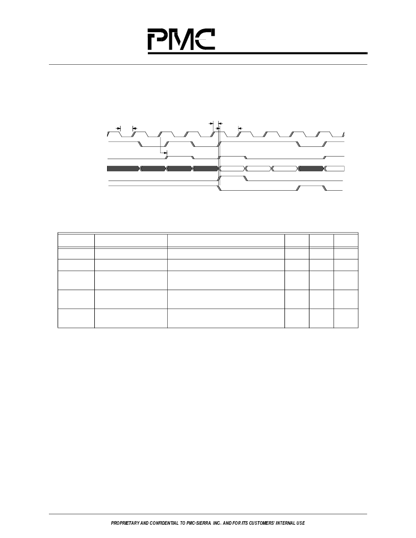
shows the data input timing for the RUTOPIA block in MPHY mode. The timing parameters used
in Figure 68 are defined in the table following the figure. Refer to
section 3.5 “Receive UTOPIA
Interface Block (RUTOPIA)” starting on page 44
for additional information.
6.5
RAM and Microprocessor Timing
6.5.1
RAM Timing
The RAM interface is designed to work with 12 ns SRAMs, which have a write data setup time of
7 ns or less, when SYS_CLK is 40 MHz (the maximum frequency). This interface is asynchro-
nous and the timing parameters are given in this section. If the interface is used at a lower fre-
quency, equations have been provided to calculate the RAM interface timing parameters. The
timing is very dependent on the pulse width of SYS_CLK. The /MEM_WE signals are derived
from the high pulse width of the SYS_CLK input. The high pulse width affects the pulse width of
/MEM_WE and the setup and hold time of MEM_DATA to the rising edge of /MEM_WE.
Refer to
section 8.6 “Board Requirements for the SRAM Interface” on page 174
for impor-
Figure 68.
RUTOPIA MPHY Timing
Symbol
Parameter
Signal
Min
Max
Unit
TPHY_CLK frequency
33
MHz
Tdc
TPHY_CLK duty cycle
45
55
%
Thd
TPHY_CLK hold time
/TPHY_ADDR, TPHY_DATA,
TPHY_SOC, /TPHY_EN
1
ns
Tq
TPHY_CLK-to-output
delay
TPHY_CLAV
12
ns
Tsu
TPHY_CLK setup time
/TPHY_ADDR, TPHY_DATA, TPHY_
SOC, /TPHY_EN
5
ns
D1
D2
D3
D4
Tq
Tsu
Thd
Tdc
TPHY_CLK(i)
/TPHY_ADDR(i)
TPHY_CLAV(o)
TPHY_DATA(i)
TPHY_SOC(i)
/TPHY_EN(i)
相關(guān)PDF資料 |
PDF描述 |
|---|---|
| PM73121-RI | AAL1 Segmentation And Reassembly Processor |
| PM73122 | 32 LINK CES/DBCES AAL1 SAR PROCESSOR |
| PM73122-BI | 32 LINK CES/DBCES AAL1 SAR PROCESSOR |
| PM73123 | 8 LINK CES/DBCES AAL1 SAR |
| PM73123-PI | 8 LINK CES/DBCES AAL1 SAR |
相關(guān)代理商/技術(shù)參數(shù) |
參數(shù)描述 |
|---|---|
| PM73121-RI | 制造商:PMC 制造商全稱:PMC 功能描述:AAL1 Segmentation And Reassembly Processor |
| PM73122 | 制造商:PMC 制造商全稱:PMC 功能描述:32 LINK CES/DBCES AAL1 SAR PROCESSOR |
| PM73122-BI | 制造商:PMC 制造商全稱:PMC 功能描述:32 LINK CES/DBCES AAL1 SAR PROCESSOR |
發(fā)布緊急采購(gòu),3分鐘左右您將得到回復(fù)。