- 您現(xiàn)在的位置:買賣IC網(wǎng) > PDF目錄69024 > MC56F8323MFB60 (FREESCALE SEMICONDUCTOR INC) 0-BIT, 120 MHz, OTHER DSP, PQFP64 PDF資料下載
參數(shù)資料
| 型號: | MC56F8323MFB60 |
| 廠商: | FREESCALE SEMICONDUCTOR INC |
| 元件分類: | 數(shù)字信號處理 |
| 英文描述: | 0-BIT, 120 MHz, OTHER DSP, PQFP64 |
| 封裝: | PLASTIC, LQFP-64 |
| 文件頁數(shù): | 76/140頁 |
| 文件大小: | 741K |
| 代理商: | MC56F8323MFB60 |
第1頁第2頁第3頁第4頁第5頁第6頁第7頁第8頁第9頁第10頁第11頁第12頁第13頁第14頁第15頁第16頁第17頁第18頁第19頁第20頁第21頁第22頁第23頁第24頁第25頁第26頁第27頁第28頁第29頁第30頁第31頁第32頁第33頁第34頁第35頁第36頁第37頁第38頁第39頁第40頁第41頁第42頁第43頁第44頁第45頁第46頁第47頁第48頁第49頁第50頁第51頁第52頁第53頁第54頁第55頁第56頁第57頁第58頁第59頁第60頁第61頁第62頁第63頁第64頁第65頁第66頁第67頁第68頁第69頁第70頁第71頁第72頁第73頁第74頁第75頁當(dāng)前第76頁第77頁第78頁第79頁第80頁第81頁第82頁第83頁第84頁第85頁第86頁第87頁第88頁第89頁第90頁第91頁第92頁第93頁第94頁第95頁第96頁第97頁第98頁第99頁第100頁第101頁第102頁第103頁第104頁第105頁第106頁第107頁第108頁第109頁第110頁第111頁第112頁第113頁第114頁第115頁第116頁第117頁第118頁第119頁第120頁第121頁第122頁第123頁第124頁第125頁第126頁第127頁第128頁第129頁第130頁第131頁第132頁第133頁第134頁第135頁第136頁第137頁第138頁第139頁第140頁
56F8323 Technical Data, Rev. 17
40
Freescale Semiconductor
Preliminary
4.7 Peripheral Memory Mapped Registers
On-chip peripheral registers are part of the data memory map on the 56800E series. These locations may
be accessed with the same addressing modes used for ordinary Data memory, except all peripheral
registers should be read/written using word accesses only.
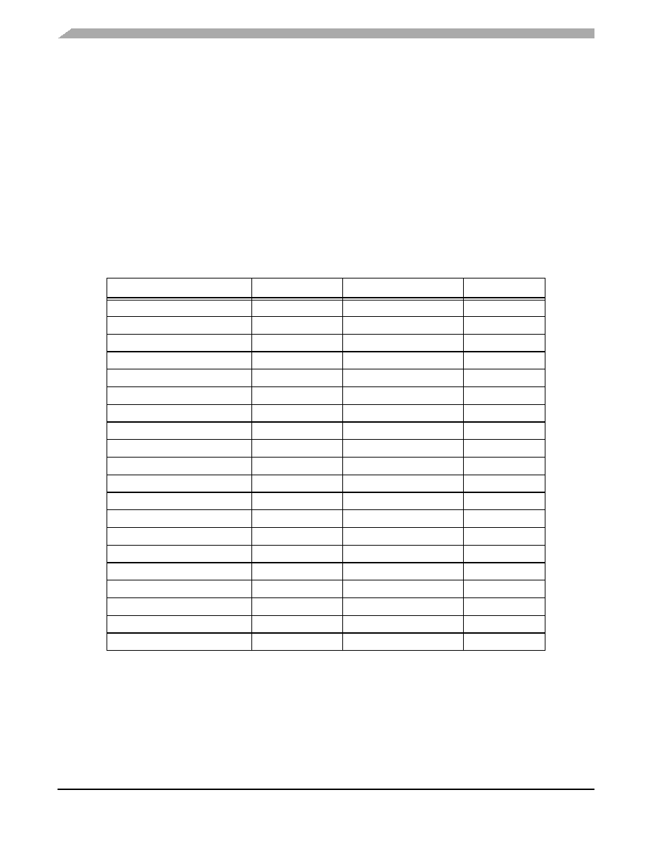
Table 4-7 summarizes base addresses for the set of peripherals on the 56F8323 and 56F8123 devices.
Peripherals are listed in order of the base address.
The following tables list all of the peripheral registers required to control or access the peripherals.
Note: Features in italics are NOT available in the 56F8123 device.
Table 4-7 Data Memory Peripheral Base Address Map Summary
Peripheral
Prefix
Base Address
Table Number
Timer A
TMRA
X:$00 F040
Timer C
TMRC
X:$00 F0C0
PWM A
PWMA
X:$00 F140
Quadrature Decoder 0
DEC0
X:$00 F180
ITCN
X:$00 F1A0
ADC A
ADCA
X:$00 F200
Temperature Sensor
TSENSOR
X:$00 F270
SCI #0
SCI0
X:$00 F280
SCI #1
SCI1
X:$00 F290
SPI #0
SPI0
X:$00 F2A0
SPI #1
SPI1
X:$00 F2B0
COP
X:$00 F2C0
PLL, OSC
CLKGEN
X:$00 F2D0
GPIO Port A
GPIOA
X:$00 F2E0
GPIO Port B
GPIOB
X:$00 F300
GPIO Port C
GPIOC
X:$00 F310
SIM
X:$00 F350
Power Supervisor
LVI
X:$00 F360
FM
X:$00 F400
FlexCAN
FC
X:$00 F800
相關(guān)PDF資料 |
PDF描述 |
|---|---|
| MC68020CFC25E | 32-BIT, 25 MHz, MICROPROCESSOR, PQFP132 |
| MC68020CFC25E | 32-BIT, 25 MHz, MICROPROCESSOR, PQFP132 |
| MC6804J1P | 8-BIT, MROM, MICROCONTROLLER, PDIP20 |
| MC6805S3VP | 8-BIT, MROM, 4.2 MHz, MICROCONTROLLER, PDIP28 |
| MC6805S3P | 8-BIT, MROM, 4.2 MHz, MICROCONTROLLER, PDIP28 |
相關(guān)代理商/技術(shù)參數(shù) |
參數(shù)描述 |
|---|---|
| MC56F8323MFBE | 功能描述:數(shù)字信號處理器和控制器 - DSP, DSC 16 BIT HYBRID CONTROLLER RoHS:否 制造商:Microchip Technology 核心:dsPIC 數(shù)據(jù)總線寬度:16 bit 程序存儲器大小:16 KB 數(shù)據(jù) RAM 大小:2 KB 最大時鐘頻率:40 MHz 可編程輸入/輸出端數(shù)量:35 定時器數(shù)量:3 設(shè)備每秒兆指令數(shù):50 MIPs 工作電源電壓:3.3 V 最大工作溫度:+ 85 C 封裝 / 箱體:TQFP-44 安裝風(fēng)格:SMD/SMT |
| MC56F8323VFB60 | 功能描述:數(shù)字信號處理器和控制器 - DSP, DSC 60MHz 60MIPS RoHS:否 制造商:Microchip Technology 核心:dsPIC 數(shù)據(jù)總線寬度:16 bit 程序存儲器大小:16 KB 數(shù)據(jù) RAM 大小:2 KB 最大時鐘頻率:40 MHz 可編程輸入/輸出端數(shù)量:35 定時器數(shù)量:3 設(shè)備每秒兆指令數(shù):50 MIPs 工作電源電壓:3.3 V 最大工作溫度:+ 85 C 封裝 / 箱體:TQFP-44 安裝風(fēng)格:SMD/SMT |
| MC56F8323VFBE | 功能描述:數(shù)字信號處理器和控制器 - DSP, DSC 16 BIT HYBRID CONTROLLER RoHS:否 制造商:Microchip Technology 核心:dsPIC 數(shù)據(jù)總線寬度:16 bit 程序存儲器大小:16 KB 數(shù)據(jù) RAM 大小:2 KB 最大時鐘頻率:40 MHz 可編程輸入/輸出端數(shù)量:35 定時器數(shù)量:3 設(shè)備每秒兆指令數(shù):50 MIPs 工作電源電壓:3.3 V 最大工作溫度:+ 85 C 封裝 / 箱體:TQFP-44 安裝風(fēng)格:SMD/SMT |
| MC56F8335 | 制造商:FREESCALE 制造商全稱:Freescale Semiconductor, Inc 功能描述:16-bit Digital Signal Controller |
| MC56F8335E | 制造商:FREESCALE 制造商全稱:Freescale Semiconductor, Inc 功能描述:16-bit Digital Signal Controller |
發(fā)布緊急采購,3分鐘左右您將得到回復(fù)。