- 您現(xiàn)在的位置:買(mǎi)賣(mài)IC網(wǎng) > PDF目錄67763 > M37920F8CGP 16-BIT, FLASH, 20 MHz, MICROCONTROLLER, PQFP100 PDF資料下載
參數(shù)資料
| 型號(hào): | M37920F8CGP |
| 元件分類(lèi): | 微控制器/微處理器 |
| 英文描述: | 16-BIT, FLASH, 20 MHz, MICROCONTROLLER, PQFP100 |
| 封裝: | 14 X 20 MM, 0.65 MM PITCH, PLASTIC, QFP-100 |
| 文件頁(yè)數(shù): | 147/155頁(yè) |
| 文件大小: | 1274K |
| 代理商: | M37920F8CGP |
第1頁(yè)第2頁(yè)第3頁(yè)第4頁(yè)第5頁(yè)第6頁(yè)第7頁(yè)第8頁(yè)第9頁(yè)第10頁(yè)第11頁(yè)第12頁(yè)第13頁(yè)第14頁(yè)第15頁(yè)第16頁(yè)第17頁(yè)第18頁(yè)第19頁(yè)第20頁(yè)第21頁(yè)第22頁(yè)第23頁(yè)第24頁(yè)第25頁(yè)第26頁(yè)第27頁(yè)第28頁(yè)第29頁(yè)第30頁(yè)第31頁(yè)第32頁(yè)第33頁(yè)第34頁(yè)第35頁(yè)第36頁(yè)第37頁(yè)第38頁(yè)第39頁(yè)第40頁(yè)第41頁(yè)第42頁(yè)第43頁(yè)第44頁(yè)第45頁(yè)第46頁(yè)第47頁(yè)第48頁(yè)第49頁(yè)第50頁(yè)第51頁(yè)第52頁(yè)第53頁(yè)第54頁(yè)第55頁(yè)第56頁(yè)第57頁(yè)第58頁(yè)第59頁(yè)第60頁(yè)第61頁(yè)第62頁(yè)第63頁(yè)第64頁(yè)第65頁(yè)第66頁(yè)第67頁(yè)第68頁(yè)第69頁(yè)第70頁(yè)第71頁(yè)第72頁(yè)第73頁(yè)第74頁(yè)第75頁(yè)第76頁(yè)第77頁(yè)第78頁(yè)第79頁(yè)第80頁(yè)第81頁(yè)第82頁(yè)第83頁(yè)第84頁(yè)第85頁(yè)第86頁(yè)第87頁(yè)第88頁(yè)第89頁(yè)第90頁(yè)第91頁(yè)第92頁(yè)第93頁(yè)第94頁(yè)第95頁(yè)第96頁(yè)第97頁(yè)第98頁(yè)第99頁(yè)第100頁(yè)第101頁(yè)第102頁(yè)第103頁(yè)第104頁(yè)第105頁(yè)第106頁(yè)第107頁(yè)第108頁(yè)第109頁(yè)第110頁(yè)第111頁(yè)第112頁(yè)第113頁(yè)第114頁(yè)第115頁(yè)第116頁(yè)第117頁(yè)第118頁(yè)第119頁(yè)第120頁(yè)第121頁(yè)第122頁(yè)第123頁(yè)第124頁(yè)第125頁(yè)第126頁(yè)第127頁(yè)第128頁(yè)第129頁(yè)第130頁(yè)第131頁(yè)第132頁(yè)第133頁(yè)第134頁(yè)第135頁(yè)第136頁(yè)第137頁(yè)第138頁(yè)第139頁(yè)第140頁(yè)第141頁(yè)第142頁(yè)第143頁(yè)第144頁(yè)第145頁(yè)第146頁(yè)當(dāng)前第147頁(yè)第148頁(yè)第149頁(yè)第150頁(yè)第151頁(yè)第152頁(yè)第153頁(yè)第154頁(yè)第155頁(yè)
91
M37920F8CGP, M37920F8CHP, M37920FCCGP
M37920FCCHP, M37920FGCGP, M37920FGCHP
PRELIMINAR
Y
Notice:
This
is not
a final
specification.
Some
parametric
limits
are
subject
to change.
SINGLE-CHIP 16-BIT CMOS MICROCOMPUTER FLASH MEMORY VERSION
MITSUBISHI MICROCOMPUTERS
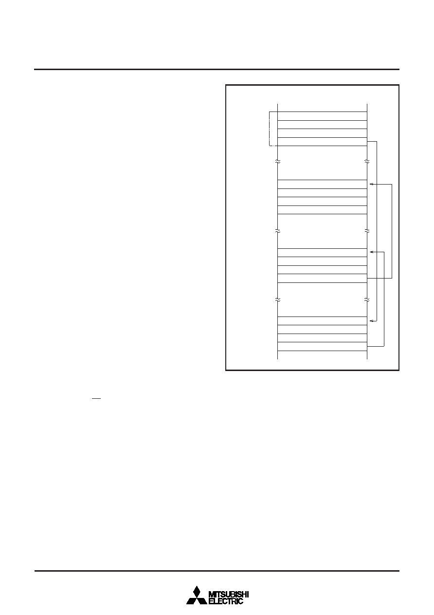
(4) Link array chain transfer mode
Figure 85 shows the perameter memory map in the link array chain
transfer mode. As shown in this figure, not only the transfer source’s
transfer start address, transfer destination’s transfer start address,
and number of transfer bytes, but also the start address of the
memory block which contains the next transfer parameters is stored.
In the transfer parameter of the last block, be sure to set “00000016”
as the start address of the next transfer parameter. For 1-bus cycle
transfer, the external I/O side’s parameters are not needed.
In the link array chain transfer, also, the DMAi mode registers L and
H, DMAi control register, and DMAC control registers L and H must
be set up. Into the SAR, write the start address of the memory block
that stores the parameters for the first transfer. This value is then
written into the TPR. Be sure that an even-numbered address is set
to the start address.
Nothing needs to be written in the DAR. Write the value 1 or more
into the TCR. When the DMA enable bit is set to “1“ after completion
of the above setup, DMA transfer becomes enabled.
In the link array chain transfer, the transfer parameters are first read
from the transfer parameter memory and then written into the SAR,
DAR, and TCR. Further, the start address of the memory block that
contains the next parameters has been written into the TPR. In the
link array chain transfer mode, the state so far is referred to as the
array state.
The DMA controller sequentially outputs the transfer parameters to
the address bus, beginning with the start address of the memory
block, storing the transfer parameters. The read data are sequen-
tially stored into the SAR, DAR, and TCR, and then the start address
of the memory block, containing the next parameters, is written into
the TPR. A DMA transfer is made in accordance with the parameters
read from the transfer parameter memory. The transfer state is the
same as in the single transfer mode. The contents of the TCR are
decremented by 1 or 2 each time when 1-transfer-unit data has been
transferred.
Even when the contents of the TCR become 0, the DMA request bit
and DMA enable bit are not cleared to “0” but the array state starts
again. When the contents of the TPR are 0 at this time, however, “L”
level is output into pin TC to clear the DMA request bit and DMA en-
able bit to “0” and terminate the link array chain transfer. At the same
timing, the interrupt request bit of the DMA interrupt control register
is set to “1”.
In the cycle steal transfer at the link array chain transfer mode, one
array state and the transfer cycle of 1 transfer unit are made by one
DMA request.
Figures 86 and 87 show timing diagram examples in the link array
chain transfer mode (burst transfer mode).
Fig. 85 Parameter memory map example in link array chain trans-
fer mode
Transfer source’s transfer start address 1
Transfer destination’s transfer start address 1
Number of transfer bytes 1
Transfer parameter address 2
Transfer source’s transfer start address 4
Transfer destination’s transfer start address 4
Number of transfer bytes 4
Transfer parameter address 5
Transfer
parameters
for
1
block
Transfer parameter
address 4
Transfer source’s transfer start address 3
Transfer destination’s transfer start address 3
Number of transfer bytes 3
Transfer parameter address 4
Transfer parameter
address 3
Transfer source’s transfer start address 2
Transfer destination’s transfer start address 2
Number of transfer bytes 2
Transfer parameter address 3
Transfer parameter
address 2
相關(guān)PDF資料 |
PDF描述 |
|---|---|
| M38039MFL-XXXHP | 8-BIT, MROM, 16.8 MHz, MICROCONTROLLER, PQFP64 |
| M38039MFL-XXXSP | 8-BIT, MROM, 16.8 MHz, MICROCONTROLLER, PDIP64 |
| M38039MFL-XXXWG | 8-BIT, MROM, 16.8 MHz, MICROCONTROLLER, PBGA64 |
| M38039FFLHP | 8-BIT, FLASH, 16.8 MHz, MICROCONTROLLER, PQFP64 |
| M38039FFLWG | 8-BIT, FLASH, 16.8 MHz, MICROCONTROLLER, PBGA64 |
相關(guān)代理商/技術(shù)參數(shù) |
參數(shù)描述 |
|---|---|
| M37920FCCGP | 制造商:MITSUBISHI 制造商全稱(chēng):Mitsubishi Electric Semiconductor 功能描述:SINGLE-CHIP 16-BIT CMOS MICROCOMPUTER FLASH MEMORY VERSION |
| M37920FCCHP | 制造商:MITSUBISHI 制造商全稱(chēng):Mitsubishi Electric Semiconductor 功能描述:SINGLE-CHIP 16-BIT CMOS MICROCOMPUTER FLASH MEMORY VERSION |
| M37920FGCGP | 制造商:MITSUBISHI 制造商全稱(chēng):Mitsubishi Electric Semiconductor 功能描述:SINGLE-CHIP 16-BIT CMOS MICROCOMPUTER FLASH MEMORY VERSION |
| M37920FGCHP | 制造商:MITSUBISHI 制造商全稱(chēng):Mitsubishi Electric Semiconductor 功能描述:SINGLE-CHIP 16-BIT CMOS MICROCOMPUTER FLASH MEMORY VERSION |
| M37920S4CGP | 制造商:MITSUBISHI 制造商全稱(chēng):Mitsubishi Electric Semiconductor 功能描述:16 BIT CMOS MICROCOMPUTER |
發(fā)布緊急采購(gòu),3分鐘左右您將得到回復(fù)。