- 您現(xiàn)在的位置:買賣IC網(wǎng) > PDF目錄67763 > M37920F8CGP 16-BIT, FLASH, 20 MHz, MICROCONTROLLER, PQFP100 PDF資料下載
參數(shù)資料
| 型號(hào): | M37920F8CGP |
| 元件分類: | 微控制器/微處理器 |
| 英文描述: | 16-BIT, FLASH, 20 MHz, MICROCONTROLLER, PQFP100 |
| 封裝: | 14 X 20 MM, 0.65 MM PITCH, PLASTIC, QFP-100 |
| 文件頁數(shù): | 115/155頁 |
| 文件大小: | 1274K |
| 代理商: | M37920F8CGP |
第1頁第2頁第3頁第4頁第5頁第6頁第7頁第8頁第9頁第10頁第11頁第12頁第13頁第14頁第15頁第16頁第17頁第18頁第19頁第20頁第21頁第22頁第23頁第24頁第25頁第26頁第27頁第28頁第29頁第30頁第31頁第32頁第33頁第34頁第35頁第36頁第37頁第38頁第39頁第40頁第41頁第42頁第43頁第44頁第45頁第46頁第47頁第48頁第49頁第50頁第51頁第52頁第53頁第54頁第55頁第56頁第57頁第58頁第59頁第60頁第61頁第62頁第63頁第64頁第65頁第66頁第67頁第68頁第69頁第70頁第71頁第72頁第73頁第74頁第75頁第76頁第77頁第78頁第79頁第80頁第81頁第82頁第83頁第84頁第85頁第86頁第87頁第88頁第89頁第90頁第91頁第92頁第93頁第94頁第95頁第96頁第97頁第98頁第99頁第100頁第101頁第102頁第103頁第104頁第105頁第106頁第107頁第108頁第109頁第110頁第111頁第112頁第113頁第114頁當(dāng)前第115頁第116頁第117頁第118頁第119頁第120頁第121頁第122頁第123頁第124頁第125頁第126頁第127頁第128頁第129頁第130頁第131頁第132頁第133頁第134頁第135頁第136頁第137頁第138頁第139頁第140頁第141頁第142頁第143頁第144頁第145頁第146頁第147頁第148頁第149頁第150頁第151頁第152頁第153頁第154頁第155頁
M37920F8CGP, M37920F8CHP, M37920FCCGP
M37920FCCHP, M37920FGCGP, M37920FGCHP
PRELIMINAR
Y
Notice:
This
is not
a final
specification.
Some
parametric
limits
are
subject
to change.
SINGLE-CHIP 16-BIT CMOS MICROCOMPUTER FLASH MEMORY VERSION
MITSUBISHI MICROCOMPUTERS
62
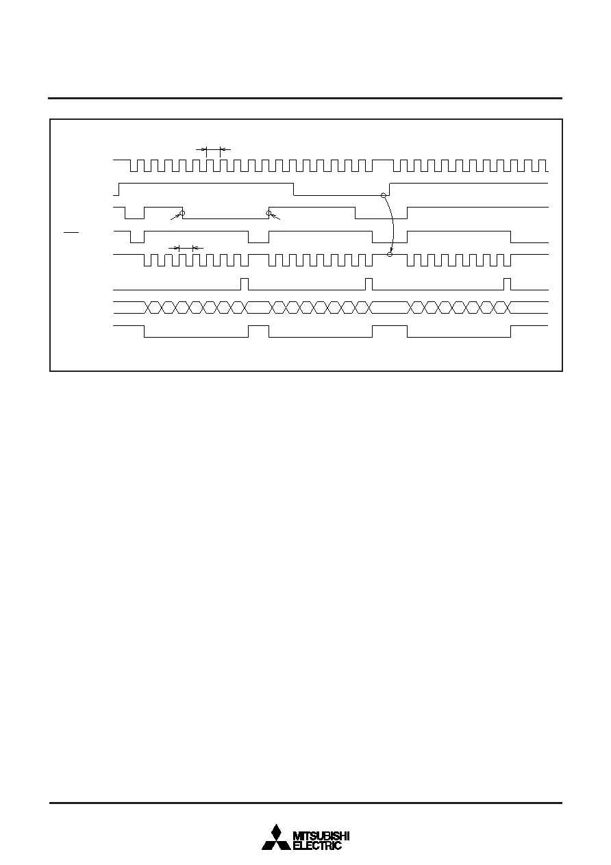
Transmission
clock
TEj
1/fi
× (n + 1) × 2
1/fi
× (n + 1) × 2
TIj
CTSj
Write in transmit buffer register
D0 D1 D2 D3 D4 D5 D6 D7
D1 D2 D3 D4 D5 D6 D7
D0 D1 D2 D3 D4 D5 D6 D7
D0
Transmit register
←Transmit buffer register
Stopped because TEj = “0”
CLKj
TENDj
TXDj
TXEPTYj
Fig. 57 Clock synchronous serial I/O timing
Interrupt request at completion of reception
When the RIk flag changes from “0” to “1”, in other words, when the
receive operation is completed, the interrupt request bit of the
UARTk receive interrupt control register can be set to “1”.
The timing when this interrupt request bit is to be set to “1” can be
selected from the following:
Each reception
When an error occurs at reception
If bit 5 of the UARTk transmit/receive control register 0 (UART re-
ceive interrupt mode select bit) is cleared to “0”, the interrupt request
bit is set to “1” at each reception. If bit 5 is set to “1”, the interrupt re-
quest bit is set to “1” only when an error occurs. (In the clock syn-
chronous serial communication, only when an overrun error occurs,
the interrupt request bit is set to “1”.)
Note that a DMA request is affected by the UART receive interrupt
mode select bit if the UARTi reception is selected as a DMA request
source of the DMA controller.
When the UARTi receive interrupt mode select bit is cleared to “0”, a
DMA request is generated at each UART reception. When the UARTi
receive interrupt mode select bit is set to “1”, a DMA request is gen-
erated only at normal UART reception. (In other words, no DMA re-
quest is generated when an error has occurred.)
Polarity of transfer clock
In the clock synchronous serial communication, by bit 6 of the UARTj
transmit/receive control register 0 (CPL), the polarity of a transfer
clock can be selected.
As shown in Figure 58, when bit 6 = “0”, the polarity is as follows:
In transmission, transmit data is output at the falling edge of CLKj.
In reception, receive data is input at the rising edge of CLKk.
When not in transfer, CLKi is at “H” level.
When bit 6 = “1”, the polarity is as follows:
In transmission, transmit data is output at the rising edge of CLKj.
In reception, receive data is input at the rising edge of CLKk.
When not in transfer, CLKi is at “L” level.
相關(guān)PDF資料 |
PDF描述 |
|---|---|
| M38039MFL-XXXHP | 8-BIT, MROM, 16.8 MHz, MICROCONTROLLER, PQFP64 |
| M38039MFL-XXXSP | 8-BIT, MROM, 16.8 MHz, MICROCONTROLLER, PDIP64 |
| M38039MFL-XXXWG | 8-BIT, MROM, 16.8 MHz, MICROCONTROLLER, PBGA64 |
| M38039FFLHP | 8-BIT, FLASH, 16.8 MHz, MICROCONTROLLER, PQFP64 |
| M38039FFLWG | 8-BIT, FLASH, 16.8 MHz, MICROCONTROLLER, PBGA64 |
相關(guān)代理商/技術(shù)參數(shù) |
參數(shù)描述 |
|---|---|
| M37920FCCGP | 制造商:MITSUBISHI 制造商全稱:Mitsubishi Electric Semiconductor 功能描述:SINGLE-CHIP 16-BIT CMOS MICROCOMPUTER FLASH MEMORY VERSION |
| M37920FCCHP | 制造商:MITSUBISHI 制造商全稱:Mitsubishi Electric Semiconductor 功能描述:SINGLE-CHIP 16-BIT CMOS MICROCOMPUTER FLASH MEMORY VERSION |
| M37920FGCGP | 制造商:MITSUBISHI 制造商全稱:Mitsubishi Electric Semiconductor 功能描述:SINGLE-CHIP 16-BIT CMOS MICROCOMPUTER FLASH MEMORY VERSION |
| M37920FGCHP | 制造商:MITSUBISHI 制造商全稱:Mitsubishi Electric Semiconductor 功能描述:SINGLE-CHIP 16-BIT CMOS MICROCOMPUTER FLASH MEMORY VERSION |
| M37920S4CGP | 制造商:MITSUBISHI 制造商全稱:Mitsubishi Electric Semiconductor 功能描述:16 BIT CMOS MICROCOMPUTER |
發(fā)布緊急采購(gòu),3分鐘左右您將得到回復(fù)。