- 您現(xiàn)在的位置:買賣IC網(wǎng) > PDF目錄67763 > M37920F8CGP 16-BIT, FLASH, 20 MHz, MICROCONTROLLER, PQFP100 PDF資料下載
參數(shù)資料
| 型號(hào): | M37920F8CGP |
| 元件分類: | 微控制器/微處理器 |
| 英文描述: | 16-BIT, FLASH, 20 MHz, MICROCONTROLLER, PQFP100 |
| 封裝: | 14 X 20 MM, 0.65 MM PITCH, PLASTIC, QFP-100 |
| 文件頁(yè)數(shù): | 114/155頁(yè) |
| 文件大?。?/td> | 1274K |
| 代理商: | M37920F8CGP |
第1頁(yè)第2頁(yè)第3頁(yè)第4頁(yè)第5頁(yè)第6頁(yè)第7頁(yè)第8頁(yè)第9頁(yè)第10頁(yè)第11頁(yè)第12頁(yè)第13頁(yè)第14頁(yè)第15頁(yè)第16頁(yè)第17頁(yè)第18頁(yè)第19頁(yè)第20頁(yè)第21頁(yè)第22頁(yè)第23頁(yè)第24頁(yè)第25頁(yè)第26頁(yè)第27頁(yè)第28頁(yè)第29頁(yè)第30頁(yè)第31頁(yè)第32頁(yè)第33頁(yè)第34頁(yè)第35頁(yè)第36頁(yè)第37頁(yè)第38頁(yè)第39頁(yè)第40頁(yè)第41頁(yè)第42頁(yè)第43頁(yè)第44頁(yè)第45頁(yè)第46頁(yè)第47頁(yè)第48頁(yè)第49頁(yè)第50頁(yè)第51頁(yè)第52頁(yè)第53頁(yè)第54頁(yè)第55頁(yè)第56頁(yè)第57頁(yè)第58頁(yè)第59頁(yè)第60頁(yè)第61頁(yè)第62頁(yè)第63頁(yè)第64頁(yè)第65頁(yè)第66頁(yè)第67頁(yè)第68頁(yè)第69頁(yè)第70頁(yè)第71頁(yè)第72頁(yè)第73頁(yè)第74頁(yè)第75頁(yè)第76頁(yè)第77頁(yè)第78頁(yè)第79頁(yè)第80頁(yè)第81頁(yè)第82頁(yè)第83頁(yè)第84頁(yè)第85頁(yè)第86頁(yè)第87頁(yè)第88頁(yè)第89頁(yè)第90頁(yè)第91頁(yè)第92頁(yè)第93頁(yè)第94頁(yè)第95頁(yè)第96頁(yè)第97頁(yè)第98頁(yè)第99頁(yè)第100頁(yè)第101頁(yè)第102頁(yè)第103頁(yè)第104頁(yè)第105頁(yè)第106頁(yè)第107頁(yè)第108頁(yè)第109頁(yè)第110頁(yè)第111頁(yè)第112頁(yè)第113頁(yè)當(dāng)前第114頁(yè)第115頁(yè)第116頁(yè)第117頁(yè)第118頁(yè)第119頁(yè)第120頁(yè)第121頁(yè)第122頁(yè)第123頁(yè)第124頁(yè)第125頁(yè)第126頁(yè)第127頁(yè)第128頁(yè)第129頁(yè)第130頁(yè)第131頁(yè)第132頁(yè)第133頁(yè)第134頁(yè)第135頁(yè)第136頁(yè)第137頁(yè)第138頁(yè)第139頁(yè)第140頁(yè)第141頁(yè)第142頁(yè)第143頁(yè)第144頁(yè)第145頁(yè)第146頁(yè)第147頁(yè)第148頁(yè)第149頁(yè)第150頁(yè)第151頁(yè)第152頁(yè)第153頁(yè)第154頁(yè)第155頁(yè)
61
M37920F8CGP, M37920F8CHP, M37920FCCGP
M37920FCCHP, M37920FGCGP, M37920FGCHP
PRELIMINAR
Y
Notice:
This
is not
a final
specification.
Some
parametric
limits
are
subject
to change.
SINGLE-CHIP 16-BIT CMOS MICROCOMPUTER FLASH MEMORY VERSION
MITSUBISHI MICROCOMPUTERS
Transmission
Transmission is started when bit 0 (TEj flag: transmit enable bit) of
UARTj transmit/receive control register 1 is “1”, bit 1 (TIj flag) of one
is “0”, and CTSj input is “L”. The TIj flag indicates whether the trans-
mit buffer register is empty or not. It is cleared to “0” when data is
written in the transmit buffer register ; it is set to “1” when the con-
tents of the transmit buffer register is transferred to the transmit reg-
ister and the transmit buffer register becomes empty.
When all of the transmit conditions are satisfied, the transmit data in
the transmit buffer register are transferred to the transmit register,
and transmission starts. As shown in Figure 57, data is output from
TXDj pin each time when transmission clock CLKj changes from “H”
to “L”. (In the clock synchronous serial I/O mode, the polarity of a
transfer clock can be changed. For details, refer to the section on the
selection of the transfer clock polarity.) The data is output from the
least significant bit.
When the transmit register becomes empty after the contents has
been transmitted, data is transferred automatically from the transmit
buffer register to the transmit register if the next transmission start
condition is satisfied. The next transmission is performed
succeedingly. Once transmission has started, the TEj flag, TIj flag,
and CTSj signals are ignored until data transmission completes.
Therefore, transmission is not interrupt when CTSj input is changed
to “H” during transmission.
The transmission start condition indicated by TEj flag, TIj flag, and
CTSj is checked while the TENDj signal (shown in Figure 57) is “H”.
Therefore, data can be transmitted continuously if the next transmis-
sion data is written in the transmit buffer register and TIj flag is
cleared to “0” before theTENDj signal goes “H”.
Bit 3 (TXEPTYj flag) of UARTj transmit/receive control register 0
changes to “1” at the next cycle just after the TENDj signal goes “H”
and changes to “0” when transmission starts. Therefore, this flag can
be used to determine whether data transmission has completed.
When the TIj flag changes from “0” to “1”, the interrupt request bit in
the UARTj transmit interrupt control register is set to “1”.
Receive
When bit 2 of the UARTk transmit/receive control register 1 is set to
“1”, reception becomes enabled. In this case, when the CLKk signal
is input, the receive operation starts simultaneously with this signal.
The RTSk output is “H” when the REK flag is “0”. When the REK flag
is set to “1”, the RTSk output becomes “L”. This informs the transmit-
ter side that reception becomes enabled. When the receive opera-
tion starts, the RTSk output automatically becomes “H”.
When the receive operation starts, the receiver takes data from pin
RxDk each time when the transmit clock (CLKj) turns from “L” to “H”.
Simultaneously with reception, the contents of the receiver register
is shifted bit by bit.
(Note that, in the clock synchronous serial communication, the polar-
ity of a transfer clock can be inverted. For details, refer to the section
on the polarity of the transfer clock.) When an 8-bit data is received,
the contents of the receive register is transferred to the receive buffer
register and bit 3 (RIk flag) of UARTk transmit/receive control regis-
ter 1 is set to “1”. In other words, the setting “1” to the RIk flag indi-
cates that the receive buffer register contains the received data. At
this time, if the low-order byte of the UARTk receive buffer register is
read out, the RTSk output turns back to “L”. This indicates that the
next data reception becomes enabled. Bit 4 (OERk flag) of UARTk
transmit/receive control register 1 is set to “1” when the next data is
transferred from the receive register to the receive buffer register
while RIk flag is “1”, and indicates that the next data was transferred
to the receive register before the contents of the receive buffer regis-
ter was read. (In other words, this indicates that an overrun error has
occurred.) RIk flag is automatically cleared to “0” when the low-order
byte of the receive buffer register is read or when the REk flag is
cleared to “0”. The OERk flag is cleared when the REk flag is
cleared. Bit 5 (FERk flag), bit 6 (PERk flag), and bit 7 (SUMk flag) are
ignored in clock synchronous mode.
As shown in Figure 50, with clock synchronous serial communica-
tion, data cannot be received unless the transmitter is operating be-
cause the receive clock is created from the transmission clock.
Therefore, the transmitter must be operating even when there is no
need to sent data from UARTk to UARTj.
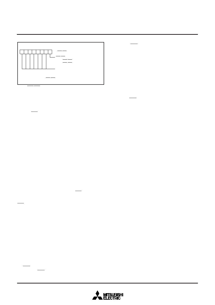
0
000
76543210
CTS/RTS separate select bit (Note)
0 : CTS/RTS are multiplexed.
1 : CTS/RTS are separate.
Must be “0”.
CTS/RTS separate select register
Address
AC16
Note: Valid when the CTS/RTS enable bit (bit 4 at address 3416) = “0”.
Fig. 56 CTS/RTS separate select register bit configuration
相關(guān)PDF資料 |
PDF描述 |
|---|---|
| M38039MFL-XXXHP | 8-BIT, MROM, 16.8 MHz, MICROCONTROLLER, PQFP64 |
| M38039MFL-XXXSP | 8-BIT, MROM, 16.8 MHz, MICROCONTROLLER, PDIP64 |
| M38039MFL-XXXWG | 8-BIT, MROM, 16.8 MHz, MICROCONTROLLER, PBGA64 |
| M38039FFLHP | 8-BIT, FLASH, 16.8 MHz, MICROCONTROLLER, PQFP64 |
| M38039FFLWG | 8-BIT, FLASH, 16.8 MHz, MICROCONTROLLER, PBGA64 |
相關(guān)代理商/技術(shù)參數(shù) |
參數(shù)描述 |
|---|---|
| M37920FCCGP | 制造商:MITSUBISHI 制造商全稱:Mitsubishi Electric Semiconductor 功能描述:SINGLE-CHIP 16-BIT CMOS MICROCOMPUTER FLASH MEMORY VERSION |
| M37920FCCHP | 制造商:MITSUBISHI 制造商全稱:Mitsubishi Electric Semiconductor 功能描述:SINGLE-CHIP 16-BIT CMOS MICROCOMPUTER FLASH MEMORY VERSION |
| M37920FGCGP | 制造商:MITSUBISHI 制造商全稱:Mitsubishi Electric Semiconductor 功能描述:SINGLE-CHIP 16-BIT CMOS MICROCOMPUTER FLASH MEMORY VERSION |
| M37920FGCHP | 制造商:MITSUBISHI 制造商全稱:Mitsubishi Electric Semiconductor 功能描述:SINGLE-CHIP 16-BIT CMOS MICROCOMPUTER FLASH MEMORY VERSION |
| M37920S4CGP | 制造商:MITSUBISHI 制造商全稱:Mitsubishi Electric Semiconductor 功能描述:16 BIT CMOS MICROCOMPUTER |
發(fā)布緊急采購(gòu),3分鐘左右您將得到回復(fù)。