- 您現(xiàn)在的位置:買賣IC網(wǎng) > PDF目錄69010 > M34502M2-XXXFP 4-BIT, MROM, MICROCONTROLLER, PDSO24 PDF資料下載
參數(shù)資料
| 型號(hào): | M34502M2-XXXFP |
| 元件分類: | 微控制器/微處理器 |
| 英文描述: | 4-BIT, MROM, MICROCONTROLLER, PDSO24 |
| 封裝: | 5.30 X 10.10 MM, 0.80 MM PITCH, PLASTIC, SSOP-24 |
| 文件頁數(shù): | 21/96頁 |
| 文件大?。?/td> | 958K |
| 代理商: | M34502M2-XXXFP |
第1頁第2頁第3頁第4頁第5頁第6頁第7頁第8頁第9頁第10頁第11頁第12頁第13頁第14頁第15頁第16頁第17頁第18頁第19頁第20頁當(dāng)前第21頁第22頁第23頁第24頁第25頁第26頁第27頁第28頁第29頁第30頁第31頁第32頁第33頁第34頁第35頁第36頁第37頁第38頁第39頁第40頁第41頁第42頁第43頁第44頁第45頁第46頁第47頁第48頁第49頁第50頁第51頁第52頁第53頁第54頁第55頁第56頁第57頁第58頁第59頁第60頁第61頁第62頁第63頁第64頁第65頁第66頁第67頁第68頁第69頁第70頁第71頁第72頁第73頁第74頁第75頁第76頁第77頁第78頁第79頁第80頁第81頁第82頁第83頁第84頁第85頁第86頁第87頁第88頁第89頁第90頁第91頁第92頁第93頁第94頁第95頁第96頁
28
Ver 1.4
MITSUBISHI MICROCOMPUTERS
7640 Group
SINGLE-CHIP 8-BIT CMOS MICROCOMPUTER
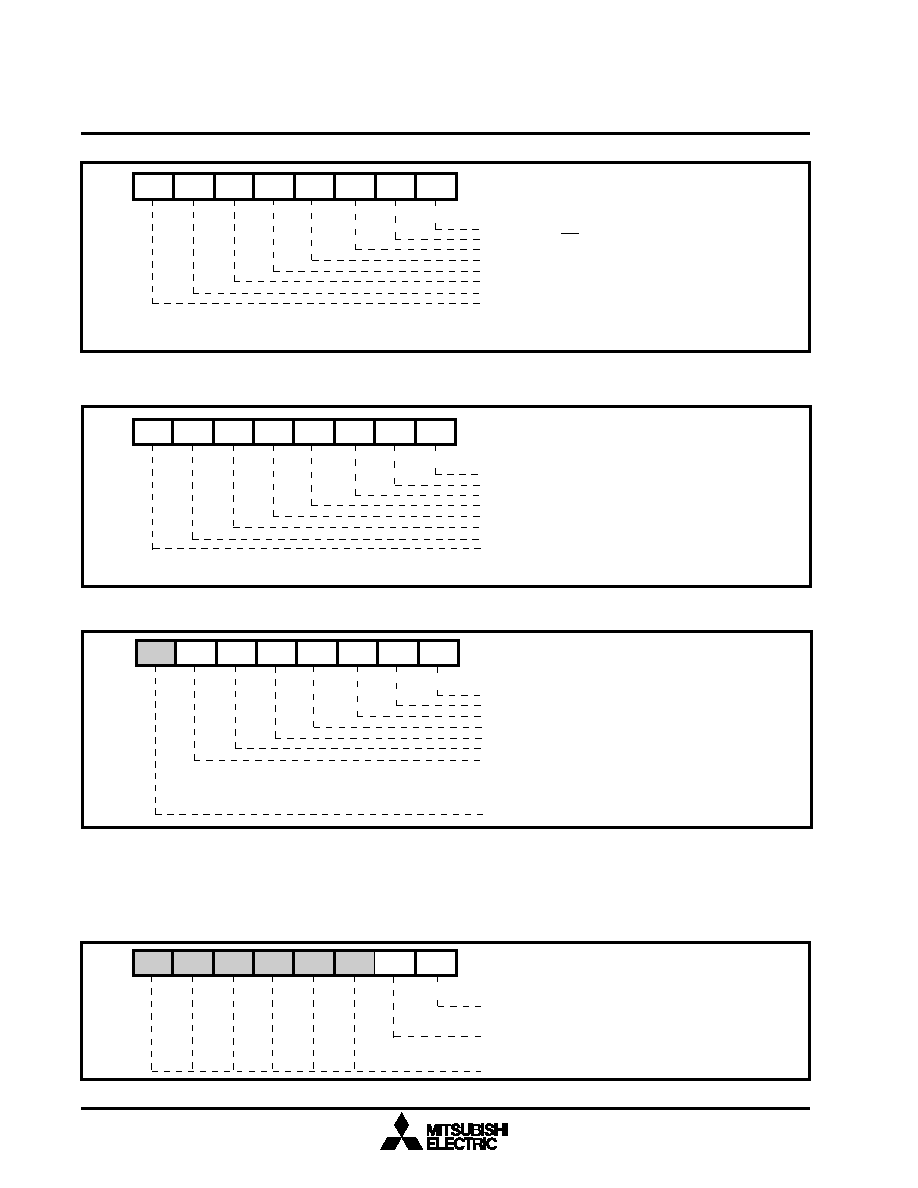
Fig. 1.30. Interrupt Polarity Register (IPOL)
Fig. 1.29. Interrupt Control Register C (ICONC)
Fig. 1.28. Interrupt Control Register B (ICONB)
Fig. 1.27 Interrupt Control Register A (ICONA)
ICA5
ICA4
ICA2
ICA1
ICA0
MSB
LSB
0
ICA3
ICA7
ICA6
ICA 0
USB Function Interrupt Enable (bit 0)
ICA 1
USB SOF Interrupt Enable (bit 1)
ICA 2
External Interrupt 0 Enable (bit 2)
ICA 3
External Interrupt 1 Enable (bit 3)
ICA 4
DMAC channel 0 Interrupt Enable (bit 4)
ICA 5
DMAC channel 1 Interrupt Enable (bit 5)
ICA 6
UART1 Receive Buffer Full Interrupt Enable (bit 6)
ICA 7
UART1 Transmit Interrupt Enable (bit 7)
0: Interrupt Disable
1: Interrupt Enable
Address: 0005
16
Access:
R/W
Reset:
00
16
The interrupt polarity register allows the user to se-
lect the edge that will trigger an external interrupt
Reserved
INT1 Pol INT0 Pol
MSB
7
LSB
0
Reserved
Address: 0011
16
Access:
R/W
Reset:
00
16
INT0 Pol
INT0 Interrupt Edge Selection Bit
0: Falling edge selected
1: Rising edge selected
INT1 Pol
INT1 Interrupt Edge Selection Bit
0: Falling edge selected
1: Rising edge selected
Bits 2-7
Reserved (Read/Write “0”)
request. The polarity register (IPOL) for the external
interrupts is shown in Figure 1.30.
ICC 0
Timer 3 Interrupt Enable (bit 0)
ICC 1
External CNTR0 Interrupt Enable (bit 1)
ICC 2
External CNTR1 Interrupt Enable (bit 2)
ICC 3
SIO Interrupt Enable (bit 3)
ICC 4
Input Buffer Full Interrupt Enable (bit 4)
ICC 5
Output Buffer Empty Interrupt Enable (bit 5)
ICC 6
Key-on Wake up Interrupt Enable (bit 6)
0: Interrupt Disable
1: Interrupt Enable
ICC 7
Reserved (Read/Write “0”)
Address: 0007
16
Access:
R/W
Reset:
00
16
ICC5
ICC4
ICC2
ICC1
ICC0
MSB
7
LSB
0
ICC3
ICC6
Reserved
ICB5
ICB4
ICB2
ICB1
ICB0
MSB
7
LSB
0
ICB3
ICB7
ICB6
ICB 0
UART1 Error Sum Interrupt Enable (bit 0)
ICB 1
UART2 Receive Buffer Full Interrupt Enable (bit 1)
ICB 2
UART2 Transmit Interrupt Enable (bit 2)
ICB 3
UART2 Error Sum Interrupt Enable (bit 3)
ICB 4
Timer X Interrupt Enable (bit 4)
ICB 5
Timer Y Interrupt Enable (bit 5)
ICB 6
Timer 1 Interrupt Enable ( bit 6)
ICB 7
Timer 2 Interrupt Enable (bit 7)
0: Interrupt Disable
1: Interrupt Enable
Address: 0006
16
Access:
R/W
Reset:
00
16
相關(guān)PDF資料 |
PDF描述 |
|---|---|
| M34502M4-XXXFP | 4-BIT, MROM, MICROCONTROLLER, PDSO24 |
| M34506M4-XXXFP | 4-BIT, MROM, MICROCONTROLLER, PDSO20 |
| M34506E4FP | 4-BIT, OTPROM, MICROCONTROLLER, PDSO20 |
| M34508G4HFP | 4-BIT, MROM, 6 MHz, MICROCONTROLLER, PDSO20 |
| M34508G4GP | 4-BIT, MROM, 6 MHz, MICROCONTROLLER, PDSO20 |
相關(guān)代理商/技術(shù)參數(shù) |
參數(shù)描述 |
|---|---|
| M34502M4 | 制造商:RENESAS 制造商全稱:Renesas Technology Corp 功能描述:SINGLE-CHIP 4-BIT CMOS MICROCOMPUTER |
| M34502M4-XXXFP | 制造商:RENESAS 制造商全稱:Renesas Technology Corp 功能描述:SINGLE-CHIP 4-BIT CMOS MICROCOMPUTER |
| M34506E4 | 制造商:RENESAS 制造商全稱:Renesas Technology Corp 功能描述:SINGLE-CHIP 4-BIT CMOS MICROCOMPUTER |
| M34506E4FP | 制造商:RENESAS 制造商全稱:Renesas Technology Corp 功能描述:SINGLE-CHIP 4-BIT CMOS MICROCOMPUTER |
| M34506M2 | 制造商:RENESAS 制造商全稱:Renesas Technology Corp 功能描述:SINGLE-CHIP 4-BIT CMOS MICROCOMPUTER |
發(fā)布緊急采購,3分鐘左右您將得到回復(fù)。