- 您現(xiàn)在的位置:買賣IC網(wǎng) > PDF目錄378513 > CY7C68001 (Cypress Semiconductor Corp.) EZ-USB FX2 USB Microcontroller High-Speed USB Peripheral Controller PDF資料下載
參數(shù)資料
| 型號: | CY7C68001 |
| 廠商: | Cypress Semiconductor Corp. |
| 元件分類: | 基準電壓源/電流源 |
| 英文描述: | EZ-USB FX2 USB Microcontroller High-Speed USB Peripheral Controller |
| 中文描述: | EZ - USB FX2的USB微控制器的高速USB外設控制器 |
| 文件頁數(shù): | 7/42頁 |
| 文件大?。?/td> | 1588K |
| 代理商: | CY7C68001 |
第1頁第2頁第3頁第4頁第5頁第6頁當前第7頁第8頁第9頁第10頁第11頁第12頁第13頁第14頁第15頁第16頁第17頁第18頁第19頁第20頁第21頁第22頁第23頁第24頁第25頁第26頁第27頁第28頁第29頁第30頁第31頁第32頁第33頁第34頁第35頁第36頁第37頁第38頁第39頁第40頁第41頁第42頁
CY7C68001
Document #: 38-08013 Rev. *H
Page 7 of 42
3.7.8
An address of [1 0 0] on FIFOADR [2:0] will select the
command interface. The command interface is used to write
to and read from the
SX2
registers and the Endpoint 0 buffer,
as well as the descriptor RAM. Command read and write trans-
actions occur over FD[7:0] only. Each byte written to the
SX2
is either an address or a data byte, as determined by bit7. If
bit7 = 1, then the byte is considered an address byte. If bit7 =
0, then the byte is considered a data byte. If bit7 = 1, then bit6
determines whether the address byte is a read request or a
write request. If bit6 = 1, then the byte is considered a read
request. If bit6 = 0 then the byte is considered a write request.
Bits [5:0] hold the register address of the request. The format
of the command address byte is shown in
Table 3-4
.
Command Protocol
Each Write request is followed by two or more data bytes. If
another address byte is received before both data bytes are
received, the
SX2
ignores the first address and any incomplete
data transfers. The format for the data bytes is shown in
Table 3-5
and
Table 3-6
. Some registers take a series of bytes.
Each byte is transferred using the same protocol.
Table 3-5. Command Data Byte One
Table 3-6. Command Data Byte Two
The first command data byte contains the upper nibble of data,
and the second command byte contains the lower nibble of
data.
3.7.8.1
Prior to writing to a register, two conditions must be met:
FIFOADR[2:0] must hold [1 0 0], and the Ready line must be
HIGH. The external master should not initiate a command if
the READY pin is not in a HIgh state.
Example
: to write the byte <10110000> into the IFCONFIG
register (0x01), first send a command address byte as follows.
Write Request Example
The first bit signifies an address transfer.
The second bit signifies that this is a write command.
The next six bits represent the register address (000001
binary = 0x01 hex).
Once the byte has been received the
SX2
pulls the READY
pin low to inform the external master not to send any more
information. When the
SX2
is ready to receive the next byte,
the
SX2
pulls the READY pin high again. This next byte, the
upper nibble of the data byte, is written to the
SX2
as follows.
The first bit signifies that this is a data transfer.
The next three are don’t care bits.
The next four bits hold the upper nibble of the transferred
byte.
Once the byte has been received the
SX2
pulls the READY
pin low to inform the external master not to send any more
information. When the
SX2
is ready to receive the next byte,
the
SX2
pulls the READY pin high again. This next byte, the
lower nibble of the data byte is written to the
SX2
.
At this point the entire byte <10110000> has been transferred
to register 0x01 and the write sequence is complete.
3.7.8.2
The Read cycle is simpler than the write cycle. The Read cycle
consists of a read request from the external master to the
SX2
.
For example, to read the contents of register 0x01, a command
address byte is written to the
SX2
as follows.
Read Request Example
When the data is ready to be read, the
SX2
asserts the INT#
pin to tell the external master that the data it requested is
waiting on FD[7:0].
[5]
Note:
5.
An important note: Once the
SX2
receives a Read request, the
SX2
allocates the interrupt line solely for the read request. If one of the six interrupt sources
described in Section 3.4 is asserted, the
SX2
will buffer that interrupt until the read request completes.
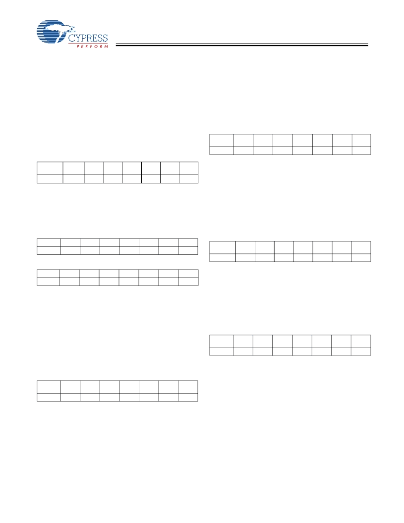
Table 3-4. Command Address Byte
Address/
Data#
Bit 7
Read/
Write#
Bit 6
A5
Bit 5
A4
Bit 4
A3
Bit 3
A2
Bit 2
A1
Bit 1
A0
Bit 0
Bit 7
Bit 6
Bit 5
Bit 4
Bit 3
Bit 2
Bit 1
Bit 0
0
X
X
X
D7
D6
D5
D4
Bit 7
Bit 6
Bit 5
Bit 4
Bit 3
Bit 2
Bit 1
Bit 0
0
X
X
X
D3
D2
D1
D0
Table 3-7. Command Address Write Byte
Address/
Data#
Read/
Write#
A5
A4
A3
A2
A1
A0
1
0
0
0
0
0
0
1
Table 3-8. Command Data Write Byte One
Address/
Data#
Don’t
Care
Don’t
Care
Don’t
Care
D7
D6
D5
D4
0
X
X
X
1
0
1
1
Table 3-9. Command Data Write Byte Two
Address/
Data#
Don’t
Care
Don’t
Care
Don’t
Care
D3
D2
D1
D0
0
X
X
X
0
0
0
0
Table 3-10. Command Address Read Byte
Address/
Data#
Read/
Write#
A5
A4
A3
A2
A1
A0
1
1
0
0
0
0
0
1
相關PDF資料 |
PDF描述 |
|---|---|
| CY7C68013 | Universal Serial Bus Microcontroller(EZ-USB FX2 USB 高速USB外圍微控制器) |
| CY7C68015A | EZ-USB FX2LP USB Microcontroller |
| CY7C68013A-100AXC | Hook-Up Wire; Conductor Size AWG:26; No. Strands x Strand Size:7 x 34; Jacket Color:Purple; Approval Bodies:UL, CSA; Approval Categories:UL AWM Styles 1007, 1565; CSA Types TR-64, TRSR-64; JQA-F; Passes VW-1 Flame Test RoHS Compliant: Yes |
| CY7C68014A-100AXC | Light Pipe; Mounting Hole Dia:3.5mm; Material:Polycarbonate; Length:10.2mm; Color:Clear; Leaded Process Compatible:Yes; Peak Reflow Compatible (260 C):Yes RoHS Compliant: Yes |
| CY7C68014A-128AXC | Light Pipe; Mounting Hole Dia:3.5mm; Material:Polycarbonate; Length:11.4mm; Color:Clear; Leaded Process Compatible:Yes; Peak Reflow Compatible (260 C):Yes RoHS Compliant: Yes |
相關代理商/技術參數(shù) |
參數(shù)描述 |
|---|---|
| CY7C68001-56LFXC | 功能描述:輸入/輸出控制器接口集成電路 8/16 Bit Datapath LO COM RoHS:否 制造商:Silicon Labs 產(chǎn)品: 輸入/輸出端數(shù)量: 工作電源電壓: 最大工作溫度:+ 85 C 最小工作溫度:- 40 C 安裝風格:SMD/SMT 封裝 / 箱體:QFN-64 封裝:Tray |
| CY7C68001-56LTXC | 功能描述:USB 接口集成電路 USB HS Controller RoHS:否 制造商:Cypress Semiconductor 產(chǎn)品:USB 2.0 數(shù)據(jù)速率: 接口類型:SPI 工作電源電壓:3.15 V to 3.45 V 工作電源電流: 最大工作溫度:+ 85 C 安裝風格:SMD/SMT 封裝 / 箱體:WLCSP-20 |
| CY7C68001-56LTXCKG | 制造商:Rochester Electronics LLC 功能描述: 制造商:Cypress Semiconductor 功能描述: |
| CY7C68001-56PVCT | 制造商:Cypress Semiconductor 功能描述:High Speed USB Interface Device 56-Pin SSOP T/R |
| CY7C68001-56PVXC | 功能描述:USB 接口集成電路 8/16 Bit Datapath LO COM RoHS:否 制造商:Cypress Semiconductor 產(chǎn)品:USB 2.0 數(shù)據(jù)速率: 接口類型:SPI 工作電源電壓:3.15 V to 3.45 V 工作電源電流: 最大工作溫度:+ 85 C 安裝風格:SMD/SMT 封裝 / 箱體:WLCSP-20 |
發(fā)布緊急采購,3分鐘左右您將得到回復。