- 您現(xiàn)在的位置:買賣IC網(wǎng) > PDF目錄378513 > CY7C68001 (Cypress Semiconductor Corp.) EZ-USB FX2 USB Microcontroller High-Speed USB Peripheral Controller PDF資料下載
參數(shù)資料
| 型號(hào): | CY7C68001 |
| 廠商: | Cypress Semiconductor Corp. |
| 元件分類: | 基準(zhǔn)電壓源/電流源 |
| 英文描述: | EZ-USB FX2 USB Microcontroller High-Speed USB Peripheral Controller |
| 中文描述: | EZ - USB FX2的USB微控制器的高速USB外設(shè)控制器 |
| 文件頁(yè)數(shù): | 15/42頁(yè) |
| 文件大?。?/td> | 1588K |
| 代理商: | CY7C68001 |
第1頁(yè)第2頁(yè)第3頁(yè)第4頁(yè)第5頁(yè)第6頁(yè)第7頁(yè)第8頁(yè)第9頁(yè)第10頁(yè)第11頁(yè)第12頁(yè)第13頁(yè)第14頁(yè)當(dāng)前第15頁(yè)第16頁(yè)第17頁(yè)第18頁(yè)第19頁(yè)第20頁(yè)第21頁(yè)第22頁(yè)第23頁(yè)第24頁(yè)第25頁(yè)第26頁(yè)第27頁(yè)第28頁(yè)第29頁(yè)第30頁(yè)第31頁(yè)第32頁(yè)第33頁(yè)第34頁(yè)第35頁(yè)第36頁(yè)第37頁(yè)第38頁(yè)第39頁(yè)第40頁(yè)第41頁(yè)第42頁(yè)
CY7C68001
Document #: 38-08013 Rev. *H
Page 15 of 42
7.1
IFCONFIG Register 0x01
7.1.1
This bit selects the clock source for the FIFOs. If IFCLKSRC =
0, the external clock on the IFCLK pin is selected. If
IFCLKSRC = 1 (default), an internal 30 or 48 MHz clock is
used.
Bit 7: IFCLKSRC
7.1.2
This bit selects the internal FIFO clock frequency. If 3048MHZ
= 0, the internal clock frequency is 30 MHz. If 3048MHZ = 1
(default), the internal clock frequency is 48 MHz.
Bit 6: 3048MHZ
7.1.3
This bit selects if the IFCLK pin is driven. If IFCLKOE = 0
(default), the IFCLK pin is floated. If IFCLKOE = 1, the IFCLK
pin is driven.
Bit 5: IFCLKOE
7.1.4
This bit controls the polarity of the IFCLK signal.
When IFCLKPOL=0, the clock has the polarity shown in all
the timing diagrams in this data sheet (rising edge is the
activating edge).
When IFCLKPOL=1, the clock is inverted (in some cases
may help with satisfying data set-up times).
Bit 4: IFCLKPOL
7.1.5
This bit controls whether the FIFO interface is synchronous or
asynchronous. When ASYNC = 0, the FIFOs operate synchro-
nously. In synchronous mode, a clock is supplied either inter-
nally or externally on the IFCLK pin, and the FIFO control
signals function as read and write enable signals for the clock
signal.
Bit 3: ASYNC
When ASYNC = 1 (default), the FIFOs operate asynchro-
nously. No clock signal input to IFCLK is required, and the
FIFO control signals function directly as read and write
strobes.
7.1.6
This bit instructs the
SX2
to enter a low-power mode. When
STANDBY=1, the
SX2
will enter a low-power mode by turning
off its oscillator. The external master should write this bit after
it receives a bus activity interrupt (indicating that the host has
signaled a USB suspend condition). If
SX2
is disconnected
from the USB bus, the external master can write this bit at any
time to save power. Once suspended, the
SX2
is awakened
either by resumption of USB bus activity or by assertion of its
WAKEUP pin.
Bit 2: STANDBY
7.1.7
This bit controls the function of the FLAGD/CS# pin. When
FLAGD/CS# = 0 (default), the pin operates as a slave chip
select. If FLAGD/CS# = 1, the pin operates as FLAGD.
Bit 1: FLAGD/CS#
7.1.8
This bit controls whether the internal pull-up resistor
connected to D+ is pulled high or floating. When DISCON = 1
(default), the pull-up resistor is floating simulating a USB
unplug. When DISCON=0, the pull-up resistor is pulled high
signaling a USB connection.
Bit 0: DISCON
7.2
The
SX2
has four FIFO flags output pins: FLAGA, FLAGB,
FLAGC, FLAGD.
FLAGSAB/FLAGSCD Registers 0x02/0x03
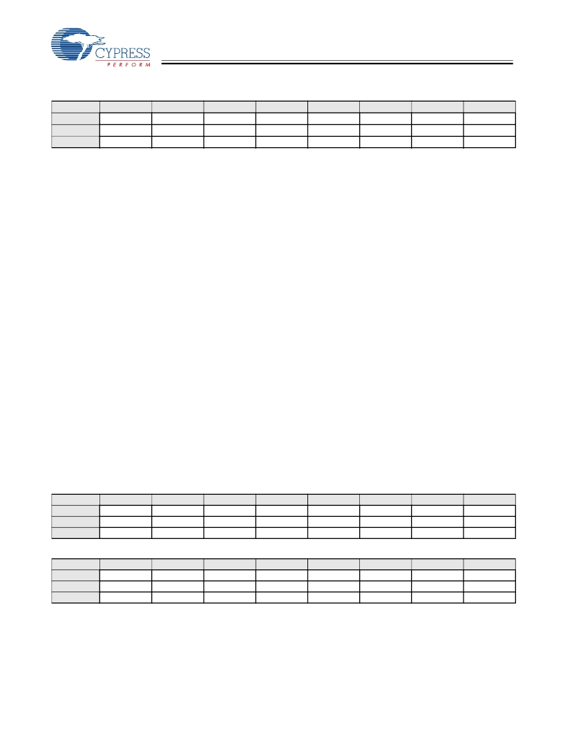
IFCONFIG
0x01
Bit #
7
6
5
4
3
2
1
0
Bit Name
IFCLKSRC
3048MHZ
IFCLKOE
IFCLKPOL
ASYNC
STANDBY
FLAGD/CS#
DISCON
Read/Write
R/W
R/W
R/W
R/W
R/W
R/W
R/W
R/W
Default
1
1
0
0
1
0
0
1
FLAGSAB
0x02
Bit #
7
6
5
4
3
2
1
0
Bit Name
FLAGB3
FLAGB2
FLAGB1
FLAGB0
FLAGA3
FLAGA2
FLAGA1
FLAGA0
Read/Write
R/W
R/W
R/W
R/W
R/W
R/W
R/W
R/W
Default
0
0
0
0
0
0
0
0
FLAGSCD
0x03
Bit #
7
6
5
4
3
2
1
0
Bit Name
FLAGD3
FLAGD2
FLAGD1
FLAGD0
FLAGC3
FLAGC2
FLAGC1
FLAGC0
Read/Write
R/W
R/W
R/W
R/W
R/W
R/W
R/W
R/W
Default
0
0
0
0
0
0
0
0
相關(guān)PDF資料 |
PDF描述 |
|---|---|
| CY7C68013 | Universal Serial Bus Microcontroller(EZ-USB FX2 USB 高速USB外圍微控制器) |
| CY7C68015A | EZ-USB FX2LP USB Microcontroller |
| CY7C68013A-100AXC | Hook-Up Wire; Conductor Size AWG:26; No. Strands x Strand Size:7 x 34; Jacket Color:Purple; Approval Bodies:UL, CSA; Approval Categories:UL AWM Styles 1007, 1565; CSA Types TR-64, TRSR-64; JQA-F; Passes VW-1 Flame Test RoHS Compliant: Yes |
| CY7C68014A-100AXC | Light Pipe; Mounting Hole Dia:3.5mm; Material:Polycarbonate; Length:10.2mm; Color:Clear; Leaded Process Compatible:Yes; Peak Reflow Compatible (260 C):Yes RoHS Compliant: Yes |
| CY7C68014A-128AXC | Light Pipe; Mounting Hole Dia:3.5mm; Material:Polycarbonate; Length:11.4mm; Color:Clear; Leaded Process Compatible:Yes; Peak Reflow Compatible (260 C):Yes RoHS Compliant: Yes |
相關(guān)代理商/技術(shù)參數(shù) |
參數(shù)描述 |
|---|---|
| CY7C68001-56LFXC | 功能描述:輸入/輸出控制器接口集成電路 8/16 Bit Datapath LO COM RoHS:否 制造商:Silicon Labs 產(chǎn)品: 輸入/輸出端數(shù)量: 工作電源電壓: 最大工作溫度:+ 85 C 最小工作溫度:- 40 C 安裝風(fēng)格:SMD/SMT 封裝 / 箱體:QFN-64 封裝:Tray |
| CY7C68001-56LTXC | 功能描述:USB 接口集成電路 USB HS Controller RoHS:否 制造商:Cypress Semiconductor 產(chǎn)品:USB 2.0 數(shù)據(jù)速率: 接口類型:SPI 工作電源電壓:3.15 V to 3.45 V 工作電源電流: 最大工作溫度:+ 85 C 安裝風(fēng)格:SMD/SMT 封裝 / 箱體:WLCSP-20 |
| CY7C68001-56LTXCKG | 制造商:Rochester Electronics LLC 功能描述: 制造商:Cypress Semiconductor 功能描述: |
| CY7C68001-56PVCT | 制造商:Cypress Semiconductor 功能描述:High Speed USB Interface Device 56-Pin SSOP T/R |
| CY7C68001-56PVXC | 功能描述:USB 接口集成電路 8/16 Bit Datapath LO COM RoHS:否 制造商:Cypress Semiconductor 產(chǎn)品:USB 2.0 數(shù)據(jù)速率: 接口類型:SPI 工作電源電壓:3.15 V to 3.45 V 工作電源電流: 最大工作溫度:+ 85 C 安裝風(fēng)格:SMD/SMT 封裝 / 箱體:WLCSP-20 |
發(fā)布緊急采購(gòu),3分鐘左右您將得到回復(fù)。