- 您現(xiàn)在的位置:買賣IC網(wǎng) > PDF目錄360516 > 7540 250MA CMOS LDO, ISUPPLY 1UA & 2% VOUT ACCURACY, -40C to +125C, 3-SOT-89, T/R PDF資料下載
參數(shù)資料
| 型號: | 7540 |
| 英文描述: | 250MA CMOS LDO, ISUPPLY 1UA & 2% VOUT ACCURACY, -40C to +125C, 3-SOT-89, T/R |
| 中文描述: | 7540群用戶手冊數(shù)據(jù)4267K/MAY.28.03 |
| 文件頁數(shù): | 241/365頁 |
| 文件大小: | 4267K |
| 代理商: | 7540 |
第1頁第2頁第3頁第4頁第5頁第6頁第7頁第8頁第9頁第10頁第11頁第12頁第13頁第14頁第15頁第16頁第17頁第18頁第19頁第20頁第21頁第22頁第23頁第24頁第25頁第26頁第27頁第28頁第29頁第30頁第31頁第32頁第33頁第34頁第35頁第36頁第37頁第38頁第39頁第40頁第41頁第42頁第43頁第44頁第45頁第46頁第47頁第48頁第49頁第50頁第51頁第52頁第53頁第54頁第55頁第56頁第57頁第58頁第59頁第60頁第61頁第62頁第63頁第64頁第65頁第66頁第67頁第68頁第69頁第70頁第71頁第72頁第73頁第74頁第75頁第76頁第77頁第78頁第79頁第80頁第81頁第82頁第83頁第84頁第85頁第86頁第87頁第88頁第89頁第90頁第91頁第92頁第93頁第94頁第95頁第96頁第97頁第98頁第99頁第100頁第101頁第102頁第103頁第104頁第105頁第106頁第107頁第108頁第109頁第110頁第111頁第112頁第113頁第114頁第115頁第116頁第117頁第118頁第119頁第120頁第121頁第122頁第123頁第124頁第125頁第126頁第127頁第128頁第129頁第130頁第131頁第132頁第133頁第134頁第135頁第136頁第137頁第138頁第139頁第140頁第141頁第142頁第143頁第144頁第145頁第146頁第147頁第148頁第149頁第150頁第151頁第152頁第153頁第154頁第155頁第156頁第157頁第158頁第159頁第160頁第161頁第162頁第163頁第164頁第165頁第166頁第167頁第168頁第169頁第170頁第171頁第172頁第173頁第174頁第175頁第176頁第177頁第178頁第179頁第180頁第181頁第182頁第183頁第184頁第185頁第186頁第187頁第188頁第189頁第190頁第191頁第192頁第193頁第194頁第195頁第196頁第197頁第198頁第199頁第200頁第201頁第202頁第203頁第204頁第205頁第206頁第207頁第208頁第209頁第210頁第211頁第212頁第213頁第214頁第215頁第216頁第217頁第218頁第219頁第220頁第221頁第222頁第223頁第224頁第225頁第226頁第227頁第228頁第229頁第230頁第231頁第232頁第233頁第234頁第235頁第236頁第237頁第238頁第239頁第240頁當(dāng)前第241頁第242頁第243頁第244頁第245頁第246頁第247頁第248頁第249頁第250頁第251頁第252頁第253頁第254頁第255頁第256頁第257頁第258頁第259頁第260頁第261頁第262頁第263頁第264頁第265頁第266頁第267頁第268頁第269頁第270頁第271頁第272頁第273頁第274頁第275頁第276頁第277頁第278頁第279頁第280頁第281頁第282頁第283頁第284頁第285頁第286頁第287頁第288頁第289頁第290頁第291頁第292頁第293頁第294頁第295頁第296頁第297頁第298頁第299頁第300頁第301頁第302頁第303頁第304頁第305頁第306頁第307頁第308頁第309頁第310頁第311頁第312頁第313頁第314頁第315頁第316頁第317頁第318頁第319頁第320頁第321頁第322頁第323頁第324頁第325頁第326頁第327頁第328頁第329頁第330頁第331頁第332頁第333頁第334頁第335頁第336頁第337頁第338頁第339頁第340頁第341頁第342頁第343頁第344頁第345頁第346頁第347頁第348頁第349頁第350頁第351頁第352頁第353頁第354頁第355頁第356頁第357頁第358頁第359頁第360頁第361頁第362頁第363頁第364頁第365頁
APPENDIX
3.1 Electrical characteristics
7540 Group User
’
s Manual
3-20
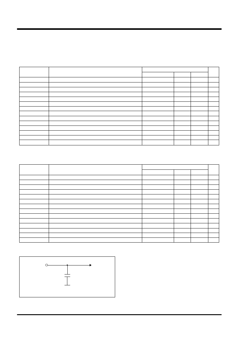
Fig. 3.1.3
Switching characteristics measurement
circuit diagram (Extended operating
temperature)
/ / /
Measured
output pin
CMOS output
100 pF
(6) Switching Characteristics (Extended operating temperature version)
Table 3.1.21 Switching characteristics (1)
(V
CC
= 4.0 to 5.5 V, V
SS
= 0 V, Ta = –40 to 85 °C, unless otherwise noted)
t
C
(S
CLK1
)/2
–
30
t
C
(S
CLK1
)/2
–
30
–
30
t
C
(S
CLK2
)/2
–
30
t
C
(S
CLK2
)/2
–
30
0
Min.
Typ.
Max.
Symbol
Parameter
Limits
Unit
t
WH
(S
CLK1
)
t
WL
(S
CLK1
)
t
d
(S
CLK1
–
TxD
1
)
t
v
(S
CLK1
–
TxD
1
)
t
r
(S
CLK1
)
t
f
(S
CLK1
)
t
WH
(S
CLK2
)
t
WL
(S
CLK2
)
t
d
(S
CLK2
–
S
DATA2
)
t
v
(S
CLK2
–
S
DATA2
)
t
r
(S
CLK2
)
t
f
(S
CLK2
)
t
r
(CMOS)
t
f
(CMOS)
Serial I/O1 clock output
“
H
”
pulse width
Serial I/O1 clock output
“
L
”
pulse width
Serial I/O1 output delay time
Serial I/O1 output valid time
Serial I/O1 clock output rising time
Serial I/O1 clock output falling time
Serial I/O2 clock output
“
H
”
pulse width
Serial I/O2 clock output
“
L
”
pulse width
Serial I/O2 output delay time
Serial I/O2 output valid time
Serial I/O2 clock output rising time
Serial I/O2 clock output falling time
CMOS output rising time (Note 1)
CMOS output falling time (Note 1)
Note 1:
Pin X
OUT
is excluded.
Table 3.1.22 Switching characteristics (2)
(V
CC
= 2.4 to 5.5 V, V
SS
= 0 V, Ta = –40 to 85 °C, unless otherwise noted)
Min.
Typ.
Max.
Symbol
Parameter
Limits
Unit
350
50
50
350
50
50
50
50
Note 1:
Pin X
OUT
is excluded.
t
WH
(S
CLK1
)
t
WL
(S
CLK1
)
t
d
(S
CLK1
–
T
x
D
1
)
t
v
(S
CLK1
–
T
x
D
1
)
t
r
(S
CLK1
)
t
f
(S
CLK1
)
t
WH
(S
CLK2
)
t
WL
(S
CLK2
)
t
d
(S
CLK2
–
S
DATA2
)
t
v
(S
CLK2
–
S
DATA2
)
t
r
(S
CLK2
)
t
f
(S
CLK2
)
t
r
(CMOS)
t
f
(CMOS)
Serial I/O1 clock output
“
H
”
pulse width
Serial I/O1 clock output
“
L
”
pulse width
Serial I/O1 output delay time
Serial I/O1 output valid time
Serial I/O1 clock output rising time
Serial I/O1 clock output falling time
Serial I/O2 clock output
“
H
”
pulse width
Serial I/O2 clock output
“
L
”
pulse width
Serial I/O2 output delay time
Serial I/O2 output valid time
Serial I/O2 clock output rising time
Serial I/O2 clock output falling time
CMOS output rising time (Note 1)
CMOS output falling time (Note 1)
t
C
(S
CLK1
)/2
–
50
t
C
(S
CLK1
)/2
–
50
–
30
t
C
(S
CLK2
)/2
–
50
t
C
(S
CLK2
)/2
–
50
0
20
20
ns
ns
ns
ns
ns
ns
ns
ns
ns
ns
ns
ns
ns
ns
10
10
140
30
30
140
30
30
30
30
ns
ns
ns
ns
ns
ns
ns
ns
ns
ns
ns
ns
ns
ns
相關(guān)PDF資料 |
PDF描述 |
|---|---|
| 7542 | 250mA CMOS LDO, lsupply 1uA and 2% Vout Accuracy, -40C to +125C, 3-SOT-23, T/R |
| 7544 | 3.3V LDO POSITVE VOLTAGE REGULATOR 2% TOL. |
| 75450PC | Peripheral IC |
| D122D | Converter IC |
| D347D | Logic IC |
相關(guān)代理商/技術(shù)參數(shù) |
參數(shù)描述 |
|---|---|
| 7540_M | 制造商:RENESAS 制造商全稱:Renesas Technology Corp 功能描述:8-BIT CISC SINGLE-CHIP MICROCOMPUTER 740 FAMILY / 740 SERIES |
| 75400 | 制造商:Honeywell Sensing and Control 功能描述: |
| 7-5-4004 | 功能描述:3M 4004 DOUBLE COATED URETHANE F 制造商:3m (tc) 系列:4004 零件狀態(tài):在售 標(biāo)準(zhǔn)包裝:1 |
| 7-5-4008 | 功能描述:3M 4008 DOUBLE COATED URETHANE F 制造商:3m (tc) 系列:4008 零件狀態(tài):在售 標(biāo)準(zhǔn)包裝:1 |
| 754010 | 制造商: 功能描述: 制造商:undefined 功能描述: |
發(fā)布緊急采購,3分鐘左右您將得到回復(fù)。