- 您現(xiàn)在的位置:買賣IC網(wǎng) > PDF目錄293971 > 5962R0150201VYC 32-BIT, 12 MHz, RISC PROCESSOR, CPGA144 PDF資料下載
參數(shù)資料
| 型號: | 5962R0150201VYC |
| 元件分類: | 微控制器/微處理器 |
| 英文描述: | 32-BIT, 12 MHz, RISC PROCESSOR, CPGA144 |
| 封裝: | CERAMIC, PGA-144 |
| 文件頁數(shù): | 15/55頁 |
| 文件大?。?/td> | 685K |
| 代理商: | 5962R0150201VYC |
第1頁第2頁第3頁第4頁第5頁第6頁第7頁第8頁第9頁第10頁第11頁第12頁第13頁第14頁當前第15頁第16頁第17頁第18頁第19頁第20頁第21頁第22頁第23頁第24頁第25頁第26頁第27頁第28頁第29頁第30頁第31頁第32頁第33頁第34頁第35頁第36頁第37頁第38頁第39頁第40頁第41頁第42頁第43頁第44頁第45頁第46頁第47頁第48頁第49頁第50頁第51頁第52頁第53頁第54頁第55頁

22
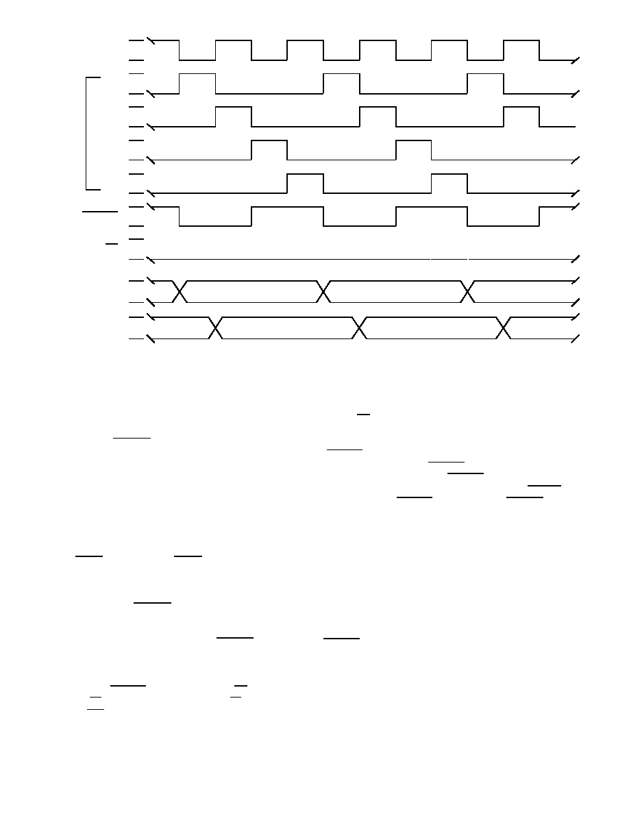
During the time period CK1, the UT1750AR begins executing
the instruction in the Primary Instruction Register (PIR). The
instruction executed is the instruction the UT1750AR fetched
during the previous bus cycle, thus the overlapping fetch and
execute cycles of the UT1750AR. During CK1, the RISC
address for the next instruction to fetch from memory becomes
valid. Also, the STATE1 output goes low, indicating the
UT1750AR is executing an instruction.
At the beginning of time period CK2, the data addressed during
CK1 becomes valid. The following conditions extend time
period CK2 one clock cycle: (1) Executing a STRI instruction,
(2) Executing a LRI instruction, or (3) Executing any instruction
with Long Immediate data. The UT1750AR also extends clock
period CK2 because of the Operand bus arbitration process. The
UT1750AR samples the logical AND combination of the Bus
Busy ( BUSY) and Bus Grant (BGNT) inverted on the falling
edge of CK2. If this combination is low during the falling edge
of CK2, time period CK2 extends until the combination of the
two signals is high, indicating the UT1750AR now controls the
Operand busses. The STATE1 output remains low for the entire
CK2 time period.
At the beginning of time period CK3, the STATE1 output goes
high indicating the next instruction is being fetched from
memory. The UT1750AR’s Operand address and data busses
become active at the beginning of CK3 along with the Bus Grant
Acknowledge ( BGACK), the Address Strobe ( AS), the Memory
or I/O (M/IO), the Operand/ Instruction (OP/IN), and the Read/
Write (R/WR ) signals.
After time period CK4 starts, the transparent latches that make
up the Primary Instruction Register open up allowing the
UT1750AR to input the instruction from RISC memory. Since
the instruction being executed requires Operand data, the Data
Strobe (DS) goes active on the falling edge of the processor
clock, one-half clock period after the rising edge of CK4. The
UT1750AR now samples the Data Transfer Acknowledge
(DTACK) signal on the next and every subsequent rising edge
of the processor clock. If DTACK is not low, the UT1750AR
extends time period CK4 until DTACK becomes active or until
an error condition is detected -- either Bus Error (BTERR) or
Memory Protect (MPROT) becomes active. STATE1 remains
high during the entire CK4 time period.
The Processor bus cycle just described is for an instruction that
requires some type of Operand data. Figure 25b shows a
UT1750AR bus cycle when no Operand data is required. This
cycle is typical of the bus cycle occurring for instructions that
only require internal processing. An example of this type of
instruction is a Move Register-to-Register instruction. For this
type of instruction, each instruction requires two processor clock
cycles for execution. Neither time period (CK2 nor CK4) is
extended because of Operand bus arbitration or a delayed
DTACK.
VALID DATA
VALID ADDRESS
VALID DATA
VALID ADDRESS
DATA
INSTRUCTION
ADDRESS
INSTRUCTION
STATE1
CK4
CK3
CK2
CK1
OSCIN
Figure 25b. Typical UT1750AR Bus Cycle
OE
相關PDF資料 |
PDF描述 |
|---|---|
| 5962R0150202VYX | 16-BIT, 16 MHz, RISC PROCESSOR, QFP132 |
| 5962R0722402VYC | SPECIALTY MICROPROCESSOR CIRCUIT, PQFP256 |
| 5962R8958702VXA | 5 V FIXED POSITIVE LDO REGULATOR, 1 V DROPOUT, CDSO16 |
| 5962R9215311VTA | 32K X 8 STANDARD SRAM, 55 ns, CDFP36 |
| 5962R9215311VTX | 32K X 8 STANDARD SRAM, 55 ns, CDFP36 |
相關代理商/技術(shù)參數(shù) |
參數(shù)描述 |
|---|---|
| 5962R0253801VZA | 制造商:Analog Devices 功能描述:- Rail/Tube |
| 5962R0720802VXC | 制造商:Texas Instruments 功能描述:ADS5463 RHA QMLV DEVICE |
| 5962R0722601VZA | 制造商:Texas Instruments 功能描述:D/A CONVERTER, 12-BIT - Trays |
| 5962R0722701VZA | 功能描述:模數(shù)轉(zhuǎn)換器 - ADC 8-Ch 50 kSPS-1 MSPS RoHS:否 制造商:Texas Instruments 通道數(shù)量:2 結(jié)構(gòu):Sigma-Delta 轉(zhuǎn)換速率:125 SPs to 8 KSPs 分辨率:24 bit 輸入類型:Differential 信噪比:107 dB 接口類型:SPI 工作電源電壓:1.7 V to 3.6 V, 2.7 V to 5.25 V 最大工作溫度:+ 85 C 安裝風格:SMD/SMT 封裝 / 箱體:VQFN-32 |
| 5962R0722902VXA | 功能描述:低壓差穩(wěn)壓器 - LDO 3-Terminal Adj Reg RoHS:否 制造商:Texas Instruments 最大輸入電壓:36 V 輸出電壓:1.4 V to 20.5 V 回動電壓(最大值):307 mV 輸出電流:1 A 負載調(diào)節(jié):0.3 % 輸出端數(shù)量: 輸出類型:Fixed 最大工作溫度:+ 125 C 安裝風格:SMD/SMT 封裝 / 箱體:VQFN-20 |
發(fā)布緊急采購,3分鐘左右您將得到回復。