- 您現(xiàn)在的位置:買賣IC網(wǎng) > PDF目錄16512 > XR17C152CM-0A-EVB (Exar Corporation)EVAL BOARD FOR XR17C152 100TQFP PDF資料下載
參數(shù)資料
| 型號: | XR17C152CM-0A-EVB |
| 廠商: | Exar Corporation |
| 文件頁數(shù): | 17/62頁 |
| 文件大?。?/td> | 0K |
| 描述: | EVAL BOARD FOR XR17C152 100TQFP |
| 標準包裝: | 1 |
| 系列: | * |
第1頁第2頁第3頁第4頁第5頁第6頁第7頁第8頁第9頁第10頁第11頁第12頁第13頁第14頁第15頁第16頁當前第17頁第18頁第19頁第20頁第21頁第22頁第23頁第24頁第25頁第26頁第27頁第28頁第29頁第30頁第31頁第32頁第33頁第34頁第35頁第36頁第37頁第38頁第39頁第40頁第41頁第42頁第43頁第44頁第45頁第46頁第47頁第48頁第49頁第50頁第51頁第52頁第53頁第54頁第55頁第56頁第57頁第58頁第59頁第60頁第61頁第62頁

XR17C152
á
5V PCI BUS DUAL UART
REV. 1.2.0
24
3.2
FIFO DATA LOADING AND UNLOADING THROUGH THE UART CHANNEL REGISTERS, THR
AND RHR IN 8-BIT FORMAT
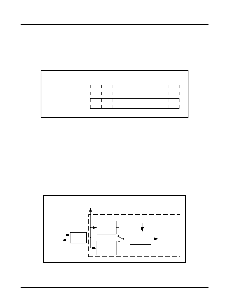
The THR and RHR register address for channel 0 to channel 1 is shown in Table 8 below. The THR and RHR
for each channel 0 tand 1 are located sequentially at address 0x0000 and 0x0200. Transmit data byte is
loaded to the THR when writing to that address and receive data is unloaded from the RHR register when
reading that address. Both THR and RHR registers are 16C550 compatible in 8-bit format, so each bus
operation can only write or read in bytes.
4.0
UART
There are 2 UARTs [channels 1:0] in the 152. Each has its own 64-byte of transmit and receive FIFO, a set of
16550 compatible control and status registers, and a baud rate generator for individual channel data rate
setting. Eight additional registers per UART were added for the EXAR enhanced features.
4.1
Programmable Baud Rate Generator
Each UART has its own Baud Rate Generator (BRG) with a prescaler for the transmitter and receiver. The
prescaler is controlled by a software bit in the MCR register. The MCR register bit-7 sets the prescaler to divide
the input crystal or external clock by 1 or 4. The output of the prescaler clocks to the BRG. The BRG further
divides this clock by a programmable divisor between 1 and (216 -1) to obtain a 16X or 8X sampling clock of
the serial data rate. The sampling clock is used by the transmitter for data bit shifting and receiver for data
sampling. The BRG divisor (DLL and DLM registers) defaults to a random value upon power up. Therefore, the
BRG must be programmed during initialization to the operating data rate.
Programming the Baud Rate Generator Registers DLM and DLL provides the capability for selecting the
operating data rate. Table 9 shows the standard data rates available with a 14.7456 MHz crystal or external
TABLE 8: TRANSMIT AND RECEIVE DATA REGISTER IN BYTE FORMAT, 16C550 COMPATIBLE
FIGURE 9. BAUD RATE GENERATOR
THR and RHR Address Locations For CH0 to CH1 (16C550 Com patible)
CH0
0x000 Write THR
CH0
0x000 Read RHR
CH1
0x200 Write THR
CH1
0x200 Read RHR
Bit-7
Bit-6
Bit-5
Bit-4
Bit-3
Bit-2
Bit-1
Bit-0
Bit-7
Bit-6
Bit-5
Bit-4
Bit-3
Bit-2
Bit-1
Bit-0
Bit-7
Bit-6
Bit-5
Bit-4
Bit-3
Bit-2
Bit-1
Bit-0
Bit-7
Bit-6
Bit-5
Bit-4
Bit-3
Bit-2
Bit-1
Bit-0
XTAL1
XTAL2
Crystal
Osc/
Buffer
MCR Bit-7=0
(default)
MCR Bit-7=1
DLL and DLM
Registers
Prescaler
Divide by 1
Prescaler
Divide by 4
16X or 8X
Sampling
Rate Clock to
Transmitter
and Receiver
To Channel 1
Baud Rate
Generator
Logic
相關(guān)PDF資料 |
PDF描述 |
|---|---|
| VE-J52-EX | CONVERTER MOD DC/DC 15V 75W |
| SI3056SSI2-EVB | BOARD EVAL SI3056/SI3010 SSI |
| 6828281-2 | CA 62.5 SC DUP-MTRJ OR SECURE |
| RHS0E152MCN1GS | CAP ALUM 1500UF 2.5V 20% SMD |
| RBM15DTKD-S288 | CONN EDGECARD 30POS .156 EXTEND |
相關(guān)代理商/技術(shù)參數(shù) |
參數(shù)描述 |
|---|---|
| XR17C152CM-F | 功能描述:UART 接口集成電路 UART RoHS:否 制造商:Texas Instruments 通道數(shù)量:2 數(shù)據(jù)速率:3 Mbps 電源電壓-最大:3.6 V 電源電壓-最小:2.7 V 電源電流:20 mA 最大工作溫度:+ 85 C 最小工作溫度:- 40 C 封裝 / 箱體:LQFP-48 封裝:Reel |
| XR17C152IM | 制造商:EXAR 制造商全稱:EXAR 功能描述:5V PCI BUS DUAL UART |
| XR17C152IM-F | 功能描述:UART 接口集成電路 UART RoHS:否 制造商:Texas Instruments 通道數(shù)量:2 數(shù)據(jù)速率:3 Mbps 電源電壓-最大:3.6 V 電源電壓-最小:2.7 V 電源電流:20 mA 最大工作溫度:+ 85 C 最小工作溫度:- 40 C 封裝 / 箱體:LQFP-48 封裝:Reel |
| XR17C154 | 制造商:EXAR 制造商全稱:EXAR 功能描述:5V PCI BUS QUAD UART |
| XR17C154_05 | 制造商:EXAR 制造商全稱:EXAR 功能描述:5V PCI BUS QUAD UART |
發(fā)布緊急采購,3分鐘左右您將得到回復。