- 您現(xiàn)在的位置:買賣IC網(wǎng) > PDF目錄140352 > W3E32M64S-200SBI (WHITE ELECTRONIC DESIGNS CORP) 32M X 64 DDR DRAM, 0.8 ns, PBGA208 PDF資料下載
參數(shù)資料
| 型號: | W3E32M64S-200SBI |
| 廠商: | WHITE ELECTRONIC DESIGNS CORP |
| 元件分類: | DRAM |
| 英文描述: | 32M X 64 DDR DRAM, 0.8 ns, PBGA208 |
| 封裝: | 13 X 22 MM, PLASTIC, BGA-208 |
| 文件頁數(shù): | 2/18頁 |
| 文件大小: | 648K |
| 代理商: | W3E32M64S-200SBI |
10
White Electronic Designs Corporation (602) 437-1520 www.whiteedc.com
White Electronic Designs
W3E32M64S-XSBX
January 2008
Rev. 6
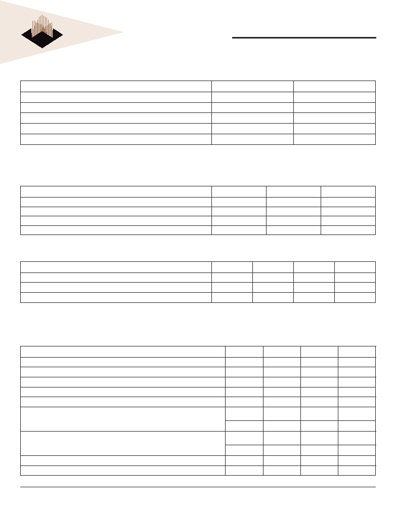
ABSOLUTE MAXIMUM RATINGS
Parameter
Unit
Voltage on VCC, VCCQ Supply relative to Vss
-1 to 3.6
V
Voltage on I/O pins relative to Vss
-1 to 3.6
V
Operating Temperature TA (Mil)
-55 to +125
°C
Operating Temperature TA (Ind)
-40 to +85
°C
Storage Temperature, Plastic
-55 to +125
°C
NOTE: Stress greater than those listed under "Absolute Maximum Ratings" may cause permanent damage to the device. This is a stress rating only and functional operation of
the device at these or any other conditions greater than those indicated in the operational sections of this specication is not implied. Exposure to absolute maximum rating
conditions for extended periods may affect reliability.
CAPACITANCE (NOTE 13)
Parameter
Symbol
Max
Unit
Input Capacitance: CK/CK#
CI1
6
pF
Addresses, BA0-1 Input Capacitance
CA
20
pF
Input Capacitance: All other input-only pins
CI2
6pF
Input/Output Capacitance: I/Os
CIO
9
pF
BGA THERMAL RESISTANCE
Description
Symbol
Typical
Units
Notes
Junction to Ambient (No Airow)
Theta JA
15.7
°C/W
1
Junction to Ball
Theta JB
13.8
°C/W
1
Junction to Case (Top)
Theta JC
2.8
°C/W
1
Refer to "PBGA Thermal Resistance Correlation" (Application Note) at www.wedc.com in the application notes section for modeling conditions.
DC ELECTRICAL CHARACTERISTICS AND OPERATING CONDITIONS
(NOTES 1-5, 16, 52)
VCC, VCCQ = +2.5V ± 0.2V; -55°C TA +125°C
Parameter/Condition
Symbol
Min
Max
Units
Supply Voltage (36, 41)
VCC
2.3
2.7
V
I/O Supply Voltage (36, 41, 44, 52)
VCCQ
2.3
2.7
V
Input Leakage Current: Any input 0V ≤ VIN ≤ VCC (All other pins not under test = 0V)
II
-2
2
μA
Input Leakage Address Current (All other pins not under test = 0V)
II
-8
8
μA
Output Leakage Current: I/Os are disabled; 0V ≤ VOUT ≤ VCCQ
IOZ
-5
5
μA
Output Levels: Full drive option (37, 39)
High Current (VOUT = VCCQ - 0.373V, minimum VREF, minimum VTT)
Low Current (VOUT = 0.373V, maximum VREF, maximum VTT)
IOH
-12
-
mA
IOL
12
-
mA
Output Levels: Reduced drive option (38, 39)
High Current (VOUT = VCCQ - 0.763V, minimum VREF, minimum VTT)
Low Current (VOUT = 0.763V, maximum VREF, maximum VTT)
IOHR
-9
-
mA
IOLR
9-
mA
I/O Reference Voltage (6,44)
VREF
0.49 x VCCQ
0.51 x VCCQ
V
I/O Termination Voltage (7, 44)
VTT
VREF - 0.04
VREF + 0.04
V
相關(guān)PDF資料 |
PDF描述 |
|---|---|
| W3EG6433S262BD4 | 32M X 64 DDR DRAM MODULE, 0.75 ns, DMA200 |
| WS57C256F-35C | 32K X 8 UVPROM, 35 ns, CQCC32 |
| WF128K32A-120HSI | 512K X 8 FLASH 12V PROM MODULE, 120 ns, CHIP66 |
| WF512K32-90HI5 | 512K X 32 FLASH 5V PROM MODULE, 90 ns, CHIP66 |
| WMF2M8-90OPM5 | 2M X 8 FLASH 5V PROM, 90 ns, CDSO56 |
相關(guān)代理商/技術(shù)參數(shù) |
參數(shù)描述 |
|---|---|
| W3E32M64S-200SBM | 制造商:Microsemi Corporation 功能描述:32M X 64 DDR, 2.5V, 200 MHZ, 208 PBGA, MIL-TEMP. - Bulk |
| W3E32M64S-250BC | 制造商:Microsemi Corporation 功能描述:32M X 64 DDR, 2.5V, 250 MHZ, 219 PBGA, COMMERCIAL TEMP. - Bulk |
| W3E32M64S-250BI | 制造商:Microsemi Corporation 功能描述:32M X 64 DDR, 2.5V, 250 MHZ, 219 PBGA, INDUSTRIAL TEMP. - Bulk |
| W3E32M64S-250BM | 制造商:Microsemi Corporation 功能描述:32M X 64 DDR, 2.5V, 250 MHZ, 219 PBGA, MIL-TEMP. - Bulk |
| W3E32M64S-250SBC | 制造商:Microsemi Corporation 功能描述:32M X 64 DDR, 2.5V, 250 MHZ, 208 PBGA, COMMERCIAL TEMP. - Bulk |
發(fā)布緊急采購,3分鐘左右您將得到回復(fù)。