- 您現(xiàn)在的位置:買賣IC網(wǎng) > PDF目錄140352 > W3E32M64S-200SBI (WHITE ELECTRONIC DESIGNS CORP) 32M X 64 DDR DRAM, 0.8 ns, PBGA208 PDF資料下載
參數(shù)資料
| 型號(hào): | W3E32M64S-200SBI |
| 廠商: | WHITE ELECTRONIC DESIGNS CORP |
| 元件分類: | DRAM |
| 英文描述: | 32M X 64 DDR DRAM, 0.8 ns, PBGA208 |
| 封裝: | 13 X 22 MM, PLASTIC, BGA-208 |
| 文件頁(yè)數(shù): | 11/18頁(yè) |
| 文件大小: | 648K |
| 代理商: | W3E32M64S-200SBI |
第1頁(yè)第2頁(yè)第3頁(yè)第4頁(yè)第5頁(yè)第6頁(yè)第7頁(yè)第8頁(yè)第9頁(yè)第10頁(yè)當(dāng)前第11頁(yè)第12頁(yè)第13頁(yè)第14頁(yè)第15頁(yè)第16頁(yè)第17頁(yè)第18頁(yè)
2
White Electronic Designs Corporation (602) 437-1520 www.whiteedc.com
White Electronic Designs
W3E32M64S-XSBX
January 2008
Rev. 6
I/O
Count
I/O
Count
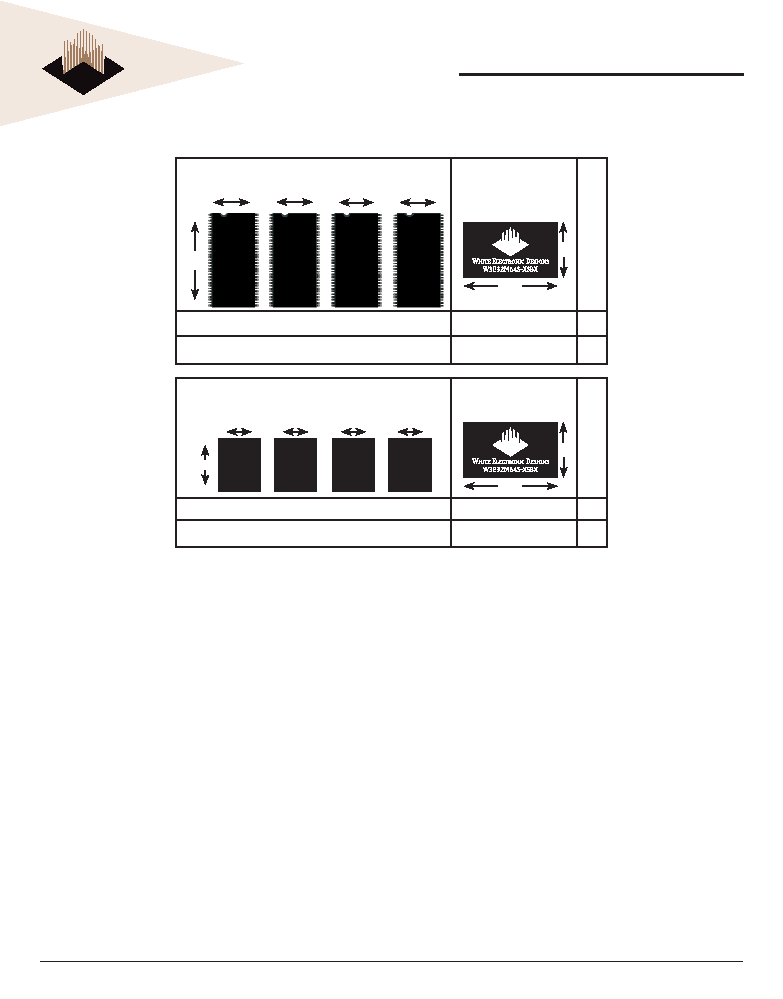
Area
4 x 265mm2 = 1060mm2
286mm2
73%
4 x 66 pins = 264 pins
208 Balls
21%
Area
4 x 125mm2 = 500mm2
286mm2
43%
4 x 60 balls = 240 balls
208 Balls
13%
S
A
V
I
N
G
S
Actual Size
W3E32M64S-XSBX
13
22
TSOP Approach (mm)
22.3
11.9
66
TSOP
66
TSOP
66
TSOP
66
TSOP
11.9
S
A
V
I
N
G
S
CSP Approach (mm)
60
FBGA
10.0
60
FBGA
10.0
60
FBGA
10.0
60
FBGA
10.0
12.5
Actual Size
W3E32M64S-XSBX
DENSITY COMPARISONS
Read and write accesses to the DDR SDRAM are burst
oriented; accesses start at a selected location and continue
for a programmed number of locations in a programmed
sequence. Accesses begin with the registration of an
ACTIVE command, which is then followed by a READ or
WRITE command. The address bits registered coincident
with the ACTIVE command are used to select the bank
and row to be accessed. The address bits registered
coincident with the READ or WRITE command are used
to select the bank and the starting column location for the
burst access.
The DDR SDRAM provides for programmable READ
or WRITE burst lengths of 2, 4, or 8 locations. An auto
precharge function may be enabled to provide a self-
timed row precharge that is initiated at the end of the
burst access.
The pipelined, multibank architecture of DDR SDRAMs
allows for concurrent operation, thereby providing high
effective bandwidth by hiding row precharge and activation
time.
An auto refresh mode is provided, along with a power-
saving power-down mode.
FUNCTIONAL DESCRIPTION
Read and write accesses to the DDR SDRAM are burst
oriented; accesses start at a selected location and continue
for a programmed number of locations in a programmed
sequence. Accesses begin with the registration of an
ACTIVE command which is then followed by a READ or
WRITE command. The address bits registered coincident
with the ACTIVE command are used to select the bank and
row to be accessed (BA0 and BA1 select the bank, A0-12
select the row). The address bits registered coincident
with the READ or WRITE command are used to select the
starting column location for the burst access.
Prior to normal operation, the DDR SDRAM must be initial-
ized. The following sections provide detailed information
covering device initialization, register denition, command
descriptions and device operation.
13
22
相關(guān)PDF資料 |
PDF描述 |
|---|---|
| W3EG6433S262BD4 | 32M X 64 DDR DRAM MODULE, 0.75 ns, DMA200 |
| WS57C256F-35C | 32K X 8 UVPROM, 35 ns, CQCC32 |
| WF128K32A-120HSI | 512K X 8 FLASH 12V PROM MODULE, 120 ns, CHIP66 |
| WF512K32-90HI5 | 512K X 32 FLASH 5V PROM MODULE, 90 ns, CHIP66 |
| WMF2M8-90OPM5 | 2M X 8 FLASH 5V PROM, 90 ns, CDSO56 |
相關(guān)代理商/技術(shù)參數(shù) |
參數(shù)描述 |
|---|---|
| W3E32M64S-200SBM | 制造商:Microsemi Corporation 功能描述:32M X 64 DDR, 2.5V, 200 MHZ, 208 PBGA, MIL-TEMP. - Bulk |
| W3E32M64S-250BC | 制造商:Microsemi Corporation 功能描述:32M X 64 DDR, 2.5V, 250 MHZ, 219 PBGA, COMMERCIAL TEMP. - Bulk |
| W3E32M64S-250BI | 制造商:Microsemi Corporation 功能描述:32M X 64 DDR, 2.5V, 250 MHZ, 219 PBGA, INDUSTRIAL TEMP. - Bulk |
| W3E32M64S-250BM | 制造商:Microsemi Corporation 功能描述:32M X 64 DDR, 2.5V, 250 MHZ, 219 PBGA, MIL-TEMP. - Bulk |
| W3E32M64S-250SBC | 制造商:Microsemi Corporation 功能描述:32M X 64 DDR, 2.5V, 250 MHZ, 208 PBGA, COMMERCIAL TEMP. - Bulk |
發(fā)布緊急采購(gòu),3分鐘左右您將得到回復(fù)。