- 您現(xiàn)在的位置:買賣IC網(wǎng) > PDF目錄300038 > TMX320DM642GNZ500 (TEXAS INSTRUMENTS INC) 64-BIT, 75.19 MHz, OTHER DSP, PBGA548 PDF資料下載
參數(shù)資料
| 型號: | TMX320DM642GNZ500 |
| 廠商: | TEXAS INSTRUMENTS INC |
| 元件分類: | 數(shù)字信號處理 |
| 英文描述: | 64-BIT, 75.19 MHz, OTHER DSP, PBGA548 |
| 封裝: | 27 X 27 MM, 1 MM PITCH, PLASTIC, BGA-548 |
| 文件頁數(shù): | 157/181頁 |
| 文件大小: | 2291K |
| 代理商: | TMX320DM642GNZ500 |
第1頁第2頁第3頁第4頁第5頁第6頁第7頁第8頁第9頁第10頁第11頁第12頁第13頁第14頁第15頁第16頁第17頁第18頁第19頁第20頁第21頁第22頁第23頁第24頁第25頁第26頁第27頁第28頁第29頁第30頁第31頁第32頁第33頁第34頁第35頁第36頁第37頁第38頁第39頁第40頁第41頁第42頁第43頁第44頁第45頁第46頁第47頁第48頁第49頁第50頁第51頁第52頁第53頁第54頁第55頁第56頁第57頁第58頁第59頁第60頁第61頁第62頁第63頁第64頁第65頁第66頁第67頁第68頁第69頁第70頁第71頁第72頁第73頁第74頁第75頁第76頁第77頁第78頁第79頁第80頁第81頁第82頁第83頁第84頁第85頁第86頁第87頁第88頁第89頁第90頁第91頁第92頁第93頁第94頁第95頁第96頁第97頁第98頁第99頁第100頁第101頁第102頁第103頁第104頁第105頁第106頁第107頁第108頁第109頁第110頁第111頁第112頁第113頁第114頁第115頁第116頁第117頁第118頁第119頁第120頁第121頁第122頁第123頁第124頁第125頁第126頁第127頁第128頁第129頁第130頁第131頁第132頁第133頁第134頁第135頁第136頁第137頁第138頁第139頁第140頁第141頁第142頁第143頁第144頁第145頁第146頁第147頁第148頁第149頁第150頁第151頁第152頁第153頁第154頁第155頁第156頁當(dāng)前第157頁第158頁第159頁第160頁第161頁第162頁第163頁第164頁第165頁第166頁第167頁第168頁第169頁第170頁第171頁第172頁第173頁第174頁第175頁第176頁第177頁第178頁第179頁第180頁第181頁
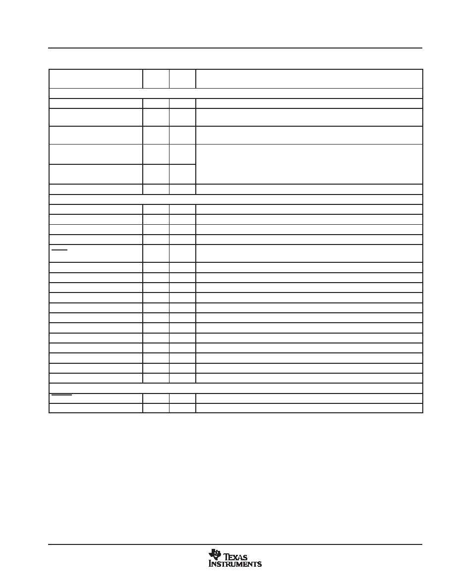
Terminal Functions
77
July 2002 Revised March 2004
SPRS200E
Table 210. Terminal Functions
SIGNAL
TYPE
IPD/
IPU
DESCRIPTION
NAME
NO.
TYPE
IPD/
IPU
DESCRIPTION
CLOCK/PLL CONFIGURATION
CLKIN
AC2
I
IPD
Clock Input. This clock is the input to the on-chip PLL.
CLKOUT4/GP0[1]§
D6
I/O/Z
IPD
Clock output at 1/4 of the device speed (O/Z) [default] or this pin can be programmed as
a GP0 1 pin (I/O/Z).
CLKOUT6/GP0[2]§
C6
I/O/Z
IPD
Clock output at 1/6 of the device speed (O/Z) [default] or this pin can be programmed as
a GP0 2 pin (I/O/Z).
CLKMODE1
AE4
I
IPD
Clock mode select
Selects whether the CPU clock frequency = input clock frequency x1 (Bypass), x6,
or x12.
CLKMODE0
AA2
I
IPD
or x12.
For more details on the CLKMODE pins and the PLL multiply factors, see the Clock
PLL section of this data sheet.
PLLV
V6
A#
PLL voltage supply
JTAG EMULATION
TMS
E15
I
IPU
JTAG test-port mode select
TDO
B18
O/Z
IPU
JTAG test-port data out
TDI
A18
I
IPU
JTAG test-port data in
TCK
A16
I
IPU
JTAG test-port clock
TRST
D14
I
IPD
JTAG test-port reset. For IEEE 1149.1 JTAG compatibility, see the IEEE 1149.1 JTAG
compatibility statement portion of this data sheet.
EMU11
D17
I/O/Z
IPU
Emulation pin 11. Reserved for future use, leave unconnected.
EMU10
C17
I/O/Z
IPU
Emulation pin 10. Reserved for future use, leave unconnected.
EMU9
B17
I/O/Z
IPU
Emulation pin 9. Reserved for future use, leave unconnected.
EMU8
D16
I/O/Z
IPU
Emulation pin 8. Reserved for future use, leave unconnected.
EMU7
A17
I/O/Z
IPU
Emulation pin 7. Reserved for future use, leave unconnected.
EMU6
C16
I/O/Z
IPU
Emulation pin 6. Reserved for future use, leave unconnected.
EMU5
B16
I/O/Z
IPU
Emulation pin 5. Reserved for future use, leave unconnected.
EMU4
D15
I/O/Z
IPU
Emulation pin 4. Reserved for future use, leave unconnected.
EMU3
C15
I/O/Z
IPU
Emulation pin 3. Reserved for future use, leave unconnected.
EMU2
B15
I/O/Z
IPU
Emulation pin 2. Reserved for future use, leave unconnected.
EMU1
C14
I/O/Z
IPU
Emulation pin 1||
EMU0
A15
I/O/Z
IPU
Emulation pin 0||
RESETS, INTERRUPTS, AND GENERAL-PURPOSE INPUT/OUTPUTS
RESET
P4
I
Device reset
NMI
B4
I
IPD
Nonmaskable interrupt, edge-driven (rising edge)
I = Input, O = Output, Z = High impedance, S = Supply voltage, GND = Ground
IPD = Internal pulldown, IPU = Internal pullup. (These IPD/IPU signal pins feature a 30-k IPD or IPU resistor. To pull up a signal to the opposite
supply rail, a 1-k
resistor should be used.)
§ These pins are multiplexed pins. For more details, see the Device Configurations section of this data sheet.
PLLV is not part of external voltage supply. See the Clock PLL section for information on how to connect this pin.
# A = Analog signal (PLL Filter)
|| The EMU0 and EMU1 pins are internally pulled up with 30-k resistors; therefore, for emulation and normal operation, no external
pullup/pulldown resistors are necessary. However, for boundary scan operation, pull down the EMU1 and EMU0 pins with a dedicated 1-k
resistor.
ADV
ANCE
INFORMA
TION
相關(guān)PDF資料 |
PDF描述 |
|---|---|
| TN4002PM | 10 MHz - 500 MHz RF/MICROWAVE WIDE BAND LOW POWER AMPLIFIER |
| TN5171PM | 20 MHz - 150 MHz RF/MICROWAVE WIDE BAND MEDIUM POWER AMPLIFIER |
| TOCP172-1MB | 970/1000 um, MULTI MODE, SIMPLEX FIBER OPTIC CONNECTOR |
| TOCP172-20CB | 970/1000 um, MULTI MODE, SIMPLEX FIBER OPTIC CONNECTOR |
| TOD5202FE | Optoelectronic |
相關(guān)代理商/技術(shù)參數(shù) |
參數(shù)描述 |
|---|---|
| TMX320DM6435AZDU | 制造商:Texas Instruments 功能描述: |
| TMX320DM6437AZDUA | 功能描述:開發(fā)板和工具包 - TMS320 Digl Media Processor RoHS:否 制造商:Texas Instruments 產(chǎn)品:Experimenter Kits 工具用于評估:F2802x 核心:TMS320 接口類型:UART, USB 工作電源電壓: |
| TMX320DM6437AZWTA | 制造商:Texas Instruments 功能描述:TMX320DM6437 PG1.1 361PIN PB-FREE NFBGA - Trays |
| TMX320DM6437BZDUA | 功能描述:數(shù)字信號處理器和控制器 - DSP, DSC Dig Media Processor RoHS:否 制造商:Microchip Technology 核心:dsPIC 數(shù)據(jù)總線寬度:16 bit 程序存儲器大小:16 KB 數(shù)據(jù) RAM 大小:2 KB 最大時鐘頻率:40 MHz 可編程輸入/輸出端數(shù)量:35 定時器數(shù)量:3 設(shè)備每秒兆指令數(shù):50 MIPs 工作電源電壓:3.3 V 最大工作溫度:+ 85 C 封裝 / 箱體:TQFP-44 安裝風(fēng)格:SMD/SMT |
| TMX320DM6437BZWTA | 功能描述:數(shù)字信號處理器和控制器 - DSP, DSC Dig Media Processor RoHS:否 制造商:Microchip Technology 核心:dsPIC 數(shù)據(jù)總線寬度:16 bit 程序存儲器大小:16 KB 數(shù)據(jù) RAM 大小:2 KB 最大時鐘頻率:40 MHz 可編程輸入/輸出端數(shù)量:35 定時器數(shù)量:3 設(shè)備每秒兆指令數(shù):50 MIPs 工作電源電壓:3.3 V 最大工作溫度:+ 85 C 封裝 / 箱體:TQFP-44 安裝風(fēng)格:SMD/SMT |
發(fā)布緊急采購,3分鐘左右您將得到回復(fù)。