- 您現(xiàn)在的位置:買賣IC網(wǎng) > PDF目錄192300 > S29PL032J65BFI150 (SPANSION LLC) 2M X 16 FLASH 3V PROM, 65 ns, PBGA56 PDF資料下載
參數(shù)資料
| 型號: | S29PL032J65BFI150 |
| 廠商: | SPANSION LLC |
| 元件分類: | PROM |
| 英文描述: | 2M X 16 FLASH 3V PROM, 65 ns, PBGA56 |
| 封裝: | 7 X 9 MM, LEAD FREE, FBGA-56 |
| 文件頁數(shù): | 65/94頁 |
| 文件大?。?/td> | 949K |
| 代理商: | S29PL032J65BFI150 |
第1頁第2頁第3頁第4頁第5頁第6頁第7頁第8頁第9頁第10頁第11頁第12頁第13頁第14頁第15頁第16頁第17頁第18頁第19頁第20頁第21頁第22頁第23頁第24頁第25頁第26頁第27頁第28頁第29頁第30頁第31頁第32頁第33頁第34頁第35頁第36頁第37頁第38頁第39頁第40頁第41頁第42頁第43頁第44頁第45頁第46頁第47頁第48頁第49頁第50頁第51頁第52頁第53頁第54頁第55頁第56頁第57頁第58頁第59頁第60頁第61頁第62頁第63頁第64頁當前第65頁第66頁第67頁第68頁第69頁第70頁第71頁第72頁第73頁第74頁第75頁第76頁第77頁第78頁第79頁第80頁第81頁第82頁第83頁第84頁第85頁第86頁第87頁第88頁第89頁第90頁第91頁第92頁第93頁第94頁
66
S29PL-J
S29PL-J_00_A8 July 29, 2005
Ad van c e
Inf o rmation
After an erase command sequence is written, if all sectors selected for erasing are protected,
DQ6 toggles for approximately 400 s, then returns to reading array data. If not all selected sec-
tors are protected, the Embedded Erase algorithm erases the unprotected sectors, and ignores
the selected sectors that are protected.
The system can use DQ6 and DQ2 together to determine whether a sector is actively erasing or
is erase-suspended. When the device is actively erasing (that is, the Embedded Erase algorithm
is in progress), DQ6 toggles. When the device enters the Erase Suspend mode, DQ6 stops tog-
gling. However, the system must also use DQ2 to determine which sectors are erasing or
erase-suspended. Alternatively, the system can use DQ7 (see the DQ7: Data# Polling).
If a program address falls within a protected sector, DQ6 toggles for approximately 1 s after
the program command sequence is written, then returns to reading array data.
DQ6 also toggles during the erase-suspend-program mode, and stops toggling once the Embed-
ded Program algorithm is complete.
differences between DQ2 and DQ6 in graphical form. See also the DQ2: Toggle Bit II.
Note: The system should recheck the toggle bit even if DQ5 = “1” because the toggle bit may stop toggling as DQ5 changes
to “1.” See the DQ6: Toggle Bit I and DQ2: Toggle Bit II for more information.
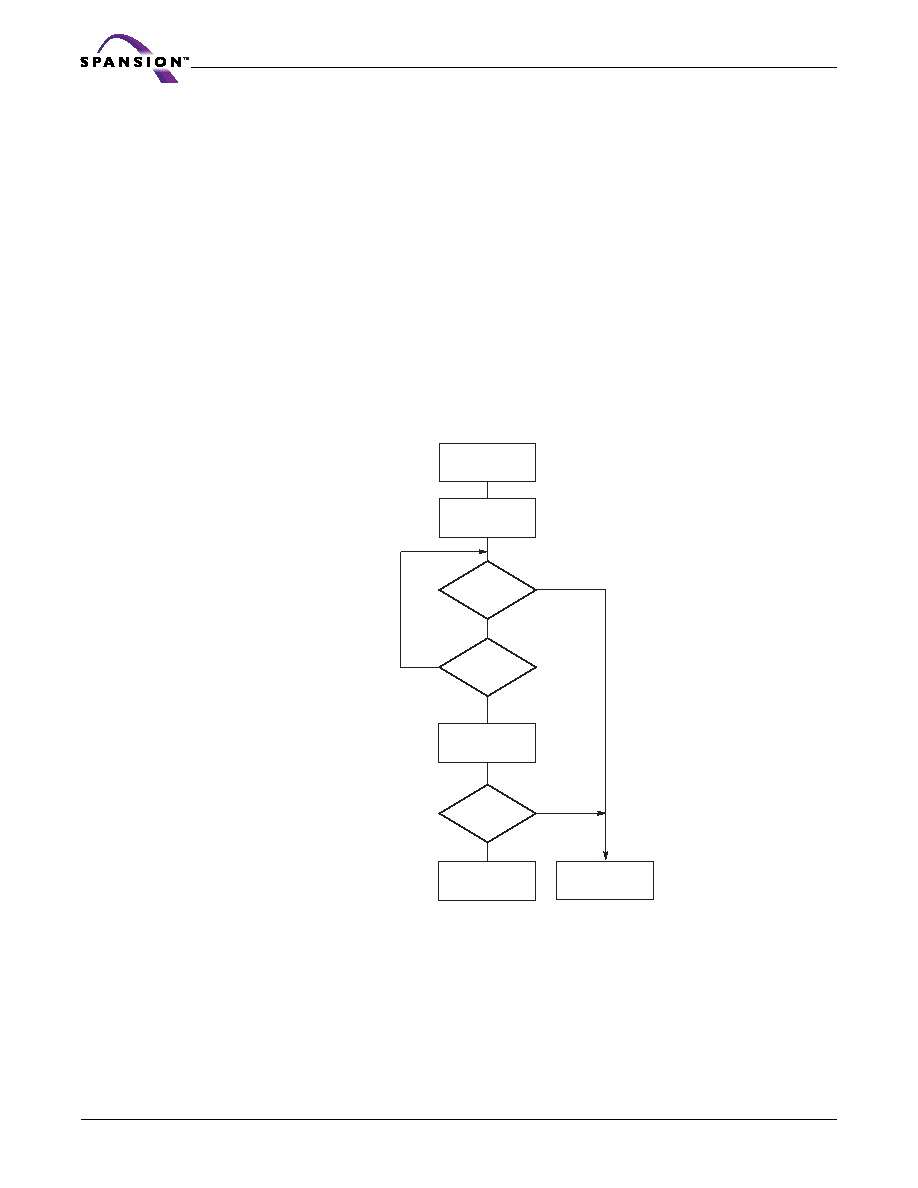
Figure 12 Toggle Bit Algorithm
DQ2: Toggle Bit II
The “Toggle Bit II” on DQ2, when used with DQ6, indicates whether a particular sector is actively
erasing (that is, the Embedded Erase algorithm is in progress), or whether that sector is
erase-suspended. Toggle Bit II is valid after the rising edge of the final WE# pulse in the com-
mand sequence.
DQ7 = Data?
Yes
No
DQ5 = 1?
No
Yes
FAIL
PASS
Read DQ7–DQ0
Addr = VA
Read DQ7–DQ0
Addr = VA
DQ7 = Data?
START
相關PDF資料 |
PDF描述 |
|---|---|
| S29PL127J70BFI000 | 8M X 16 FLASH 3V PROM, 70 ns, PBGA80 |
| S29XS064R0PBHW010 | 4M X 16 FLASH 1.8V PROM, 80 ns, PBGA44 |
| S2C3R-1-12-H | 4000 MHz - 12000 MHz RF/MICROWAVE SGL POLE DOUBLE THROW SWITCH, 2 dB INSERTION LOSS |
| S2C5R-1-12-RC | 4000 MHz - 18000 MHz RF/MICROWAVE SGL POLE DOUBLE THROW SWITCH, 2.8 dB INSERTION LOSS |
| S2H3R-1H | 10 MHz - 1000 MHz RF/MICROWAVE SGL POLE DOUBLE THROW SWITCH, 1.2 dB INSERTION LOSS |
相關代理商/技術參數(shù) |
參數(shù)描述 |
|---|---|
| S29PL032J70BAI120 | 功能描述:閃存 32Mb 3V 70ns Parallel NOR 閃存 RoHS:否 制造商:ON Semiconductor 數(shù)據(jù)總線寬度:1 bit 存儲類型:Flash 存儲容量:2 MB 結(jié)構(gòu):256 K x 8 定時類型: 接口類型:SPI 訪問時間: 電源電壓-最大:3.6 V 電源電壓-最小:2.3 V 最大工作電流:15 mA 工作溫度:- 40 C to + 85 C 安裝風格:SMD/SMT 封裝 / 箱體: 封裝:Reel |
| S29PL032J70BAI122 | 功能描述:閃存 32MB 閃存 3V 70ns Parallel NOR 閃存 RoHS:否 制造商:ON Semiconductor 數(shù)據(jù)總線寬度:1 bit 存儲類型:Flash 存儲容量:2 MB 結(jié)構(gòu):256 K x 8 定時類型: 接口類型:SPI 訪問時間: 電源電壓-最大:3.6 V 電源電壓-最小:2.3 V 最大工作電流:15 mA 工作溫度:- 40 C to + 85 C 安裝風格:SMD/SMT 封裝 / 箱體: 封裝:Reel |
| S29PL032J70BAW120 | 功能描述:閃存 32MB 閃存 3V 70ns Parallel NOR 閃存 RoHS:否 制造商:ON Semiconductor 數(shù)據(jù)總線寬度:1 bit 存儲類型:Flash 存儲容量:2 MB 結(jié)構(gòu):256 K x 8 定時類型: 接口類型:SPI 訪問時間: 電源電壓-最大:3.6 V 電源電壓-最小:2.3 V 最大工作電流:15 mA 工作溫度:- 40 C to + 85 C 安裝風格:SMD/SMT 封裝 / 箱體: 封裝:Reel |
| S29PL032J70BFI120 | 功能描述:閃存 32Mb 3V 70ns Parallel NOR 閃存 RoHS:否 制造商:ON Semiconductor 數(shù)據(jù)總線寬度:1 bit 存儲類型:Flash 存儲容量:2 MB 結(jié)構(gòu):256 K x 8 定時類型: 接口類型:SPI 訪問時間: 電源電壓-最大:3.6 V 電源電壓-最小:2.3 V 最大工作電流:15 mA 工作溫度:- 40 C to + 85 C 安裝風格:SMD/SMT 封裝 / 箱體: 封裝:Reel |
| S29PL032J70BFI120(E) | 制造商:Spansion 功能描述:Cut Tape |
發(fā)布緊急采購,3分鐘左右您將得到回復。