- 您現(xiàn)在的位置:買賣IC網(wǎng) > PDF目錄192300 > S29PL032J65BFI150 (SPANSION LLC) 2M X 16 FLASH 3V PROM, 65 ns, PBGA56 PDF資料下載
參數(shù)資料
| 型號(hào): | S29PL032J65BFI150 |
| 廠商: | SPANSION LLC |
| 元件分類: | PROM |
| 英文描述: | 2M X 16 FLASH 3V PROM, 65 ns, PBGA56 |
| 封裝: | 7 X 9 MM, LEAD FREE, FBGA-56 |
| 文件頁(yè)數(shù): | 64/94頁(yè) |
| 文件大小: | 949K |
| 代理商: | S29PL032J65BFI150 |
第1頁(yè)第2頁(yè)第3頁(yè)第4頁(yè)第5頁(yè)第6頁(yè)第7頁(yè)第8頁(yè)第9頁(yè)第10頁(yè)第11頁(yè)第12頁(yè)第13頁(yè)第14頁(yè)第15頁(yè)第16頁(yè)第17頁(yè)第18頁(yè)第19頁(yè)第20頁(yè)第21頁(yè)第22頁(yè)第23頁(yè)第24頁(yè)第25頁(yè)第26頁(yè)第27頁(yè)第28頁(yè)第29頁(yè)第30頁(yè)第31頁(yè)第32頁(yè)第33頁(yè)第34頁(yè)第35頁(yè)第36頁(yè)第37頁(yè)第38頁(yè)第39頁(yè)第40頁(yè)第41頁(yè)第42頁(yè)第43頁(yè)第44頁(yè)第45頁(yè)第46頁(yè)第47頁(yè)第48頁(yè)第49頁(yè)第50頁(yè)第51頁(yè)第52頁(yè)第53頁(yè)第54頁(yè)第55頁(yè)第56頁(yè)第57頁(yè)第58頁(yè)第59頁(yè)第60頁(yè)第61頁(yè)第62頁(yè)第63頁(yè)當(dāng)前第64頁(yè)第65頁(yè)第66頁(yè)第67頁(yè)第68頁(yè)第69頁(yè)第70頁(yè)第71頁(yè)第72頁(yè)第73頁(yè)第74頁(yè)第75頁(yè)第76頁(yè)第77頁(yè)第78頁(yè)第79頁(yè)第80頁(yè)第81頁(yè)第82頁(yè)第83頁(yè)第84頁(yè)第85頁(yè)第86頁(yè)第87頁(yè)第88頁(yè)第89頁(yè)第90頁(yè)第91頁(yè)第92頁(yè)第93頁(yè)第94頁(yè)
July 29, 2005 S29PL-J_00_A8
S29PL-J
65
Advance
Information
Notes:
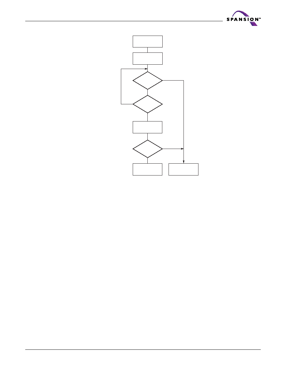
1. VA = Valid address for programming. During a sector erase operation, a valid address is any sector address within the
sector being erased. During chip erase, a valid address is any non-protected sector address.
2. DQ7 should be rechecked even if DQ5 = “1” because DQ7 may change simultaneously with DQ5.
Figure 11 Data# Polling Algorithm
RY/BY#: Ready/Busy#
The RY/BY# is a dedicated, open-drain output pin which indicates whether an Embedded Algo-
rithm is in progress or complete. The RY/BY# status is valid after the rising edge of the final WE#
pulse in the command sequence. Since RY/BY# is an open-drain output, several RY/BY# pins can
be tied together in parallel with a pull-up resistor to VCC.
If the output is low (Busy), the device is actively erasing or programming. (This includes pro-
gramming in the Erase Suspend mode.) If the output is high (Ready), the device is in the read
mode, the standby mode, or one of the banks is in the erase-suspend-read mode.
Table 23 shows the outputs for RY/BY#.
DQ6: Toggle Bit I
Toggle Bit I on DQ6 indicates whether an Embedded Program or Erase algorithm is in progress
or complete, or whether the device has entered the Erase Suspend mode. Toggle Bit I may be
read at any address, and is valid after the rising edge of the final WE# pulse in the command
sequence (prior to the program or erase operation), and during the sector erase time-out.
During an Embedded Program or Erase algorithm operation, successive read cycles to any ad-
dress cause DQ6 to toggle. The system may use either OE# or CE# to control the read cycles.
When the operation is complete, DQ6 stops toggling.
DQ7 = Data?
Yes
No
DQ5 = 1?
No
Yes
FAIL
PASS
Read DQ7–DQ0
Addr = VA
Read DQ7–DQ0
Addr = VA
DQ7 = Data?
START
相關(guān)PDF資料 |
PDF描述 |
|---|---|
| S29PL127J70BFI000 | 8M X 16 FLASH 3V PROM, 70 ns, PBGA80 |
| S29XS064R0PBHW010 | 4M X 16 FLASH 1.8V PROM, 80 ns, PBGA44 |
| S2C3R-1-12-H | 4000 MHz - 12000 MHz RF/MICROWAVE SGL POLE DOUBLE THROW SWITCH, 2 dB INSERTION LOSS |
| S2C5R-1-12-RC | 4000 MHz - 18000 MHz RF/MICROWAVE SGL POLE DOUBLE THROW SWITCH, 2.8 dB INSERTION LOSS |
| S2H3R-1H | 10 MHz - 1000 MHz RF/MICROWAVE SGL POLE DOUBLE THROW SWITCH, 1.2 dB INSERTION LOSS |
相關(guān)代理商/技術(shù)參數(shù) |
參數(shù)描述 |
|---|---|
| S29PL032J70BAI120 | 功能描述:閃存 32Mb 3V 70ns Parallel NOR 閃存 RoHS:否 制造商:ON Semiconductor 數(shù)據(jù)總線寬度:1 bit 存儲(chǔ)類型:Flash 存儲(chǔ)容量:2 MB 結(jié)構(gòu):256 K x 8 定時(shí)類型: 接口類型:SPI 訪問(wèn)時(shí)間: 電源電壓-最大:3.6 V 電源電壓-最小:2.3 V 最大工作電流:15 mA 工作溫度:- 40 C to + 85 C 安裝風(fēng)格:SMD/SMT 封裝 / 箱體: 封裝:Reel |
| S29PL032J70BAI122 | 功能描述:閃存 32MB 閃存 3V 70ns Parallel NOR 閃存 RoHS:否 制造商:ON Semiconductor 數(shù)據(jù)總線寬度:1 bit 存儲(chǔ)類型:Flash 存儲(chǔ)容量:2 MB 結(jié)構(gòu):256 K x 8 定時(shí)類型: 接口類型:SPI 訪問(wèn)時(shí)間: 電源電壓-最大:3.6 V 電源電壓-最小:2.3 V 最大工作電流:15 mA 工作溫度:- 40 C to + 85 C 安裝風(fēng)格:SMD/SMT 封裝 / 箱體: 封裝:Reel |
| S29PL032J70BAW120 | 功能描述:閃存 32MB 閃存 3V 70ns Parallel NOR 閃存 RoHS:否 制造商:ON Semiconductor 數(shù)據(jù)總線寬度:1 bit 存儲(chǔ)類型:Flash 存儲(chǔ)容量:2 MB 結(jié)構(gòu):256 K x 8 定時(shí)類型: 接口類型:SPI 訪問(wèn)時(shí)間: 電源電壓-最大:3.6 V 電源電壓-最小:2.3 V 最大工作電流:15 mA 工作溫度:- 40 C to + 85 C 安裝風(fēng)格:SMD/SMT 封裝 / 箱體: 封裝:Reel |
| S29PL032J70BFI120 | 功能描述:閃存 32Mb 3V 70ns Parallel NOR 閃存 RoHS:否 制造商:ON Semiconductor 數(shù)據(jù)總線寬度:1 bit 存儲(chǔ)類型:Flash 存儲(chǔ)容量:2 MB 結(jié)構(gòu):256 K x 8 定時(shí)類型: 接口類型:SPI 訪問(wèn)時(shí)間: 電源電壓-最大:3.6 V 電源電壓-最小:2.3 V 最大工作電流:15 mA 工作溫度:- 40 C to + 85 C 安裝風(fēng)格:SMD/SMT 封裝 / 箱體: 封裝:Reel |
| S29PL032J70BFI120(E) | 制造商:Spansion 功能描述:Cut Tape |
發(fā)布緊急采購(gòu),3分鐘左右您將得到回復(fù)。