- 您現(xiàn)在的位置:買賣IC網(wǎng) > PDF目錄369957 > PD6710 (Intel Corp.) ISA-to-PC-Card (PCMCIA) Controllers PDF資料下載
參數(shù)資料
| 型號: | PD6710 |
| 廠商: | Intel Corp. |
| 英文描述: | ISA-to-PC-Card (PCMCIA) Controllers |
| 中文描述: | ISA -到- PC卡(PCMCIA)的控制器 |
| 文件頁數(shù): | 80/138頁 |
| 文件大小: | 723K |
| 代理商: | PD6710 |
第1頁第2頁第3頁第4頁第5頁第6頁第7頁第8頁第9頁第10頁第11頁第12頁第13頁第14頁第15頁第16頁第17頁第18頁第19頁第20頁第21頁第22頁第23頁第24頁第25頁第26頁第27頁第28頁第29頁第30頁第31頁第32頁第33頁第34頁第35頁第36頁第37頁第38頁第39頁第40頁第41頁第42頁第43頁第44頁第45頁第46頁第47頁第48頁第49頁第50頁第51頁第52頁第53頁第54頁第55頁第56頁第57頁第58頁第59頁第60頁第61頁第62頁第63頁第64頁第65頁第66頁第67頁第68頁第69頁第70頁第71頁第72頁第73頁第74頁第75頁第76頁第77頁第78頁第79頁當前第80頁第81頁第82頁第83頁第84頁第85頁第86頁第87頁第88頁第89頁第90頁第91頁第92頁第93頁第94頁第95頁第96頁第97頁第98頁第99頁第100頁第101頁第102頁第103頁第104頁第105頁第106頁第107頁第108頁第109頁第110頁第111頁第112頁第113頁第114頁第115頁第116頁第117頁第118頁第119頁第120頁第121頁第122頁第123頁第124頁第125頁第126頁第127頁第128頁第129頁第130頁第131頁第132頁第133頁第134頁第135頁第136頁第137頁第138頁

PD6710/
’
22
—
ISA-to-PC-Card (PCMCIA) Controllers
80
Datasheet
During a DMA data transfer process, an ISA-based system typically follows its issuance of a DMA
acknowledge with a DMA read or write cycle. However, during a DMA write-verify operation, a
system can issue a DMA acknowledge without following it with a DMA read or write cycle.
Because a DMA-capable PC Card receives DMA acknowledgment only by reception of a DMA
read or write cycle, conditions may occur where the card never receives a DMA acknowledge. To
prevent this from happening in an ISA-based system, a maximum DMA acknowledge delay feature
has been added that generates a
‘
dummy
’
DMA write cycle (reads DMA data from the card) if
there are no system-generated DMA read or write cycles to the card within a programmable time.
Once a DMA acknowledge is received from the system, the PD6722 starts counting the time from
the assertion of the DACK* signal until the system issues a DMA read or write command (IOR* or
IOW*). If this interval exceeds the programmed time, the PD6722 assumes that a system write-
verify is in progress and generates a dummy DMA write cycle at the PC Card interface. This allows
the passing of the DMA acknowledge (and terminal count status) to the card so it can perform any
intended verify-cycle functions.
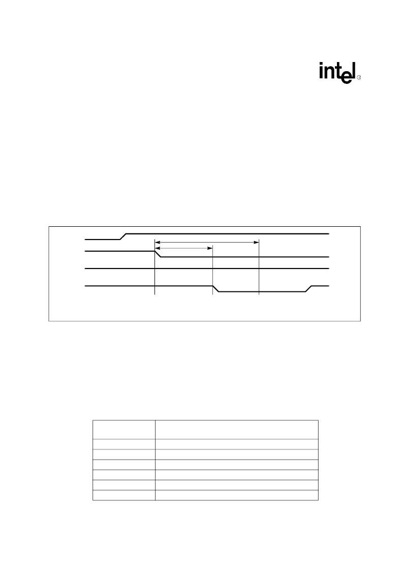
The maximum DMA acknowledge delay (t2 as shown in
Figure 12
) should be programmed to a
time greater than the maximum time required from the system
’
s issuance of a DMA acknowledge
to its issuance of a DMA read or write cycle (t1 as shown in
Figure 12
). The t1 time is indicated in
the specifications for the systems DMA cycle timing.
Typical system specifications for t1 are 190
–
270 ns, making a value of 80h for the
Maximum
DMA Acknowledge Delay
register suitable for many applications. If the PD6722 is used in an
add-in card application, a value of 20h may be suitable.
Table 14
shows
Maximum DMA
Acknowledge Delay
register values to be programmed for a desired maximum DMA acknowledge
delay.
Figure 12. Selection of Acknowledge Time-out Interval
DREQ
DACK*
AEN
IOR*/IOW*
t2
t1
t1 = time delay from DMA acknowledge to IOR* or IOW* command (specified by system design).
t2 = time to program into the Maximum DMA Acknowledge Delay register for when IOR* or IOW* falling edge does not occur (t2 > t1).
Table 14. Maximum DMA Acknowledge Delay Register Values
(Sheet 1 of 2)
Register Value
Maximum DMA Acknowledge Delay
(25-MHz internal clock and default Setup timing)
80h
7 clocks = 280 ns
40h
8 clocks = 320 ns
C0h
9 clocks = 360 ns
20h
10 clocks = 400 ns
A0h
11 clocks = 440 ns
60h
12 clocks = 480 ns
相關(guān)PDF資料 |
PDF描述 |
|---|---|
| PD7-20-70A | Analog IC |
| PD7-80-70A | Analog IC |
| PD7-40-70A | Analog IC |
| PD700A7 | Optoelectronic |
| PDA2446-B-AP | Analog Pigtailed PIN Photodiodes |
相關(guān)代理商/技術(shù)參數(shù) |
參數(shù)描述 |
|---|---|
| PD67108AM | 制造商:MICROSEMI 制造商全稱:Microsemi Corporation 功能描述:24-Channel PoE AF and AT DIMM |
| PD67108MAC-0212 | 制造商:Microsemi Corporation 功能描述:POE PSE MODULES - Bulk |
| PD67108MAC-GGGG | 制造商:MICROSEMI 制造商全稱:Microsemi Corporation 功能描述:24-Channel PoE AF and AT DIMM |
| PD67108MDC-0212 | 制造商:Microsemi Corporation 功能描述:POE PSE MODULES - Bulk |
| PD67108MDC-GGGG | 制造商:MICROSEMI 制造商全稱:Microsemi Corporation 功能描述:24-Channel PoE AF and AT DIMM |
發(fā)布緊急采購,3分鐘左右您將得到回復(fù)。