- 您現(xiàn)在的位置:買賣IC網(wǎng) > PDF目錄359141 > MC68HC08SR12 (飛思卡爾半導(dǎo)體(中國)有限公司) M68HC08 Microcontrollers PDF資料下載
參數(shù)資料
| 型號: | MC68HC08SR12 |
| 廠商: | 飛思卡爾半導(dǎo)體(中國)有限公司 |
| 英文描述: | M68HC08 Microcontrollers |
| 中文描述: | M68HC08系列微控制器 |
| 文件頁數(shù): | 399/404頁 |
| 文件大?。?/td> | 1666K |
| 代理商: | MC68HC08SR12 |
第1頁第2頁第3頁第4頁第5頁第6頁第7頁第8頁第9頁第10頁第11頁第12頁第13頁第14頁第15頁第16頁第17頁第18頁第19頁第20頁第21頁第22頁第23頁第24頁第25頁第26頁第27頁第28頁第29頁第30頁第31頁第32頁第33頁第34頁第35頁第36頁第37頁第38頁第39頁第40頁第41頁第42頁第43頁第44頁第45頁第46頁第47頁第48頁第49頁第50頁第51頁第52頁第53頁第54頁第55頁第56頁第57頁第58頁第59頁第60頁第61頁第62頁第63頁第64頁第65頁第66頁第67頁第68頁第69頁第70頁第71頁第72頁第73頁第74頁第75頁第76頁第77頁第78頁第79頁第80頁第81頁第82頁第83頁第84頁第85頁第86頁第87頁第88頁第89頁第90頁第91頁第92頁第93頁第94頁第95頁第96頁第97頁第98頁第99頁第100頁第101頁第102頁第103頁第104頁第105頁第106頁第107頁第108頁第109頁第110頁第111頁第112頁第113頁第114頁第115頁第116頁第117頁第118頁第119頁第120頁第121頁第122頁第123頁第124頁第125頁第126頁第127頁第128頁第129頁第130頁第131頁第132頁第133頁第134頁第135頁第136頁第137頁第138頁第139頁第140頁第141頁第142頁第143頁第144頁第145頁第146頁第147頁第148頁第149頁第150頁第151頁第152頁第153頁第154頁第155頁第156頁第157頁第158頁第159頁第160頁第161頁第162頁第163頁第164頁第165頁第166頁第167頁第168頁第169頁第170頁第171頁第172頁第173頁第174頁第175頁第176頁第177頁第178頁第179頁第180頁第181頁第182頁第183頁第184頁第185頁第186頁第187頁第188頁第189頁第190頁第191頁第192頁第193頁第194頁第195頁第196頁第197頁第198頁第199頁第200頁第201頁第202頁第203頁第204頁第205頁第206頁第207頁第208頁第209頁第210頁第211頁第212頁第213頁第214頁第215頁第216頁第217頁第218頁第219頁第220頁第221頁第222頁第223頁第224頁第225頁第226頁第227頁第228頁第229頁第230頁第231頁第232頁第233頁第234頁第235頁第236頁第237頁第238頁第239頁第240頁第241頁第242頁第243頁第244頁第245頁第246頁第247頁第248頁第249頁第250頁第251頁第252頁第253頁第254頁第255頁第256頁第257頁第258頁第259頁第260頁第261頁第262頁第263頁第264頁第265頁第266頁第267頁第268頁第269頁第270頁第271頁第272頁第273頁第274頁第275頁第276頁第277頁第278頁第279頁第280頁第281頁第282頁第283頁第284頁第285頁第286頁第287頁第288頁第289頁第290頁第291頁第292頁第293頁第294頁第295頁第296頁第297頁第298頁第299頁第300頁第301頁第302頁第303頁第304頁第305頁第306頁第307頁第308頁第309頁第310頁第311頁第312頁第313頁第314頁第315頁第316頁第317頁第318頁第319頁第320頁第321頁第322頁第323頁第324頁第325頁第326頁第327頁第328頁第329頁第330頁第331頁第332頁第333頁第334頁第335頁第336頁第337頁第338頁第339頁第340頁第341頁第342頁第343頁第344頁第345頁第346頁第347頁第348頁第349頁第350頁第351頁第352頁第353頁第354頁第355頁第356頁第357頁第358頁第359頁第360頁第361頁第362頁第363頁第364頁第365頁第366頁第367頁第368頁第369頁第370頁第371頁第372頁第373頁第374頁第375頁第376頁第377頁第378頁第379頁第380頁第381頁第382頁第383頁第384頁第385頁第386頁第387頁第388頁第389頁第390頁第391頁第392頁第393頁第394頁第395頁第396頁第397頁第398頁當(dāng)前第399頁第400頁第401頁第402頁第403頁第404頁
MC68HC08SR12
MC68HC908SR12MC68HC08SR12 — Rev. 5.0
Data Sheet
Freescale Semiconductor
MC68HC08SR12
399
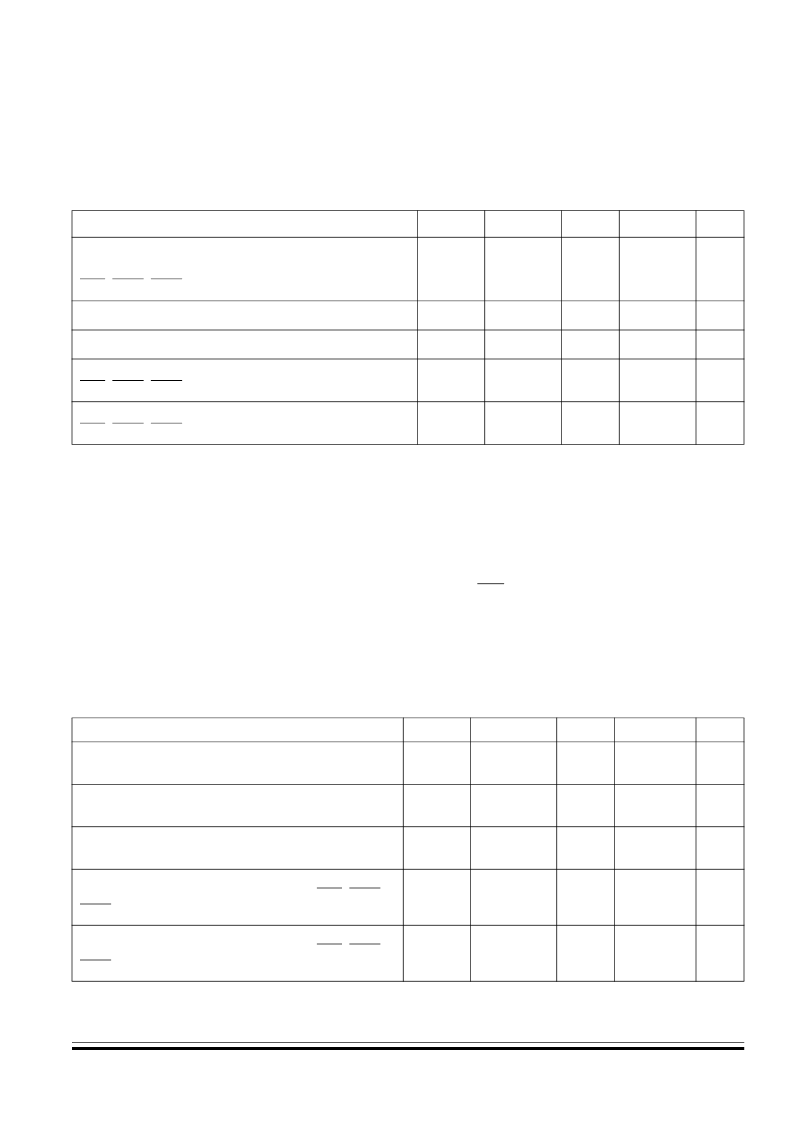
A.8.2 3.0V DC Electrical Characteristics
Pullup resistors
(8)
PTD[0:7] configured as KBI[0:7]
RST, IRQ1, IRQ2
R
PU1
R
PU2
24
24
35
35
42
42
k
k
Low-voltage inhibit, trip falling voltage
V
LVII5
3.80
4.15
4.45
V
Low-voltage inhibit, trip rising voltage
V
LVII5
3.95
4.30
4.60
V
Schmitt trigger input low level trip voltage
RST, IRQ1, IRQ2, KBI[0:7]
V
SCMTL
—
1.21
—
V
Schmitt trigger input high level trip voltage
RST, IRQ1, IRQ2, KBI[0:7]
V
SCMTH
—
1.65
—
V
Notes
:
1. V
DD
= 4.5 to 5.5 Vdc, V
SS
= 0 Vdc, T
A
= T
L
to T
H
, unless otherwise noted.
2. Typical values reflect average measurements at midpoint of voltage range, 25
°
C only.
3. Run (operating) I
DD
measured using external square wave clock source. All inputs 0.2 V from rail. No dc loads. Less than
100 pF on all outputs. C
L
= 20 pF on OSC2. All ports configured as inputs. OSC2 capacitance linearly affects run I
DD
.
Measured with all modules enabled.
4. Wait I
DD
measured using external square wave clock source. All inputs 0.2 V from rail. No dc loads. Less than 100 pF on
all outputs. C
L
= 20 pF on OSC2. All ports configured as inputs. OSC2 capacitance linearly affects wait I
DD
.
5. STOP I
DD
measured with OSC1 grounded, no port pins sourcing current.
6. Maximum is highest voltage that POR is guaranteed.
7. If minimum V
DD
is not reached before the internal POR reset is released,
RST
must be driven low externally until minimum
V
DD
is reached.
8. R
PU1
and
R
PU2
are measured at
V
DD
= 5.0V
Table A-3. 3V DC Electrical Characteristics
Characteristic
(1)
Symbol
Min
Typ
(2)
Max
Unit
Output high voltage (I
LOAD
= –1.0mA)
PTA[0:7], PTB[4:6], PTC[0:7], PTD[0:7]
V
OH
V
DD
–0.4
—
—
V
Output low voltage (I
LOAD
= 0.8mA)
PTA[0:7], PTB[0:6], PTC[0:7], PTD[0:7]
V
OL
—
—
0.4
V
LED sink current (V
Drain
= 2.0V)
PTA[0:5], PTC[3:7]
V
OL
—
–5
—
mA
Input high voltage
PTA[0:7], PTB[0:6], PTC[0:7], PTD[0:7], RST, IRQ1,
IRQ2, OSC1
V
IH
0.7
×
V
DD
—
V
DD
V
Input low voltage
PTA[0:7], PTB[0:6], PTC[0:7], PTD[0:7], RST, IRQ1,
IRQ2, OSC1
V
IL
V
SS
—
0.3
×
V
DD
V
Table A-2. 5V DC Electrical Characteristics
Characteristic
(1)
Symbol
Min
Typ
(2)
Max
Unit
相關(guān)PDF資料 |
PDF描述 |
|---|---|
| MC68HC11E0 | HC11 Microcontrollers |
| MC68HC11K0 | HCMOS Microcontroller Unit |
| MC68HC11KMNPEVS | Microcontrollers |
| MC68HC705C8AC | Microcontrollers |
| MC68HC705E6 | HCMOS Microcontroller Unit |
相關(guān)代理商/技術(shù)參數(shù) |
參數(shù)描述 |
|---|---|
| MC68HC08TV24CFB | 制造商:FREESCALE 制造商全稱:Freescale Semiconductor, Inc 功能描述:M68HC08 Microcontrollers |
| MC68HC08XL36 | 制造商:FREESCALE 制造商全稱:Freescale Semiconductor, Inc 功能描述:HCMOS Microcontroller Unit |
| MC68HC08XL36CB | 制造商:FREESCALE 制造商全稱:Freescale Semiconductor, Inc 功能描述:HCMOS Microcontroller Unit |
| MC68HC08XL36CFU | 制造商:FREESCALE 制造商全稱:Freescale Semiconductor, Inc 功能描述:HCMOS Microcontroller Unit |
| MC68HC11 | 制造商:MOTOROLA 制造商全稱:Motorola, Inc 功能描述:Port Replacement Unit (PRU) |
發(fā)布緊急采購,3分鐘左右您將得到回復(fù)。