- 您現(xiàn)在的位置:買賣IC網(wǎng) > PDF目錄69025 > MC68CK338CPV14 (FREESCALE SEMICONDUCTOR INC) 32-BIT, 14.4 MHz, MICROCONTROLLER, PQFP144 PDF資料下載
參數(shù)資料
| 型號(hào): | MC68CK338CPV14 |
| 廠商: | FREESCALE SEMICONDUCTOR INC |
| 元件分類: | 微控制器/微處理器 |
| 英文描述: | 32-BIT, 14.4 MHz, MICROCONTROLLER, PQFP144 |
| 封裝: | PLASTIC, TQFP-144 |
| 文件頁(yè)數(shù): | 62/133頁(yè) |
| 文件大小: | 944K |
| 代理商: | MC68CK338CPV14 |
第1頁(yè)第2頁(yè)第3頁(yè)第4頁(yè)第5頁(yè)第6頁(yè)第7頁(yè)第8頁(yè)第9頁(yè)第10頁(yè)第11頁(yè)第12頁(yè)第13頁(yè)第14頁(yè)第15頁(yè)第16頁(yè)第17頁(yè)第18頁(yè)第19頁(yè)第20頁(yè)第21頁(yè)第22頁(yè)第23頁(yè)第24頁(yè)第25頁(yè)第26頁(yè)第27頁(yè)第28頁(yè)第29頁(yè)第30頁(yè)第31頁(yè)第32頁(yè)第33頁(yè)第34頁(yè)第35頁(yè)第36頁(yè)第37頁(yè)第38頁(yè)第39頁(yè)第40頁(yè)第41頁(yè)第42頁(yè)第43頁(yè)第44頁(yè)第45頁(yè)第46頁(yè)第47頁(yè)第48頁(yè)第49頁(yè)第50頁(yè)第51頁(yè)第52頁(yè)第53頁(yè)第54頁(yè)第55頁(yè)第56頁(yè)第57頁(yè)第58頁(yè)第59頁(yè)第60頁(yè)第61頁(yè)當(dāng)前第62頁(yè)第63頁(yè)第64頁(yè)第65頁(yè)第66頁(yè)第67頁(yè)第68頁(yè)第69頁(yè)第70頁(yè)第71頁(yè)第72頁(yè)第73頁(yè)第74頁(yè)第75頁(yè)第76頁(yè)第77頁(yè)第78頁(yè)第79頁(yè)第80頁(yè)第81頁(yè)第82頁(yè)第83頁(yè)第84頁(yè)第85頁(yè)第86頁(yè)第87頁(yè)第88頁(yè)第89頁(yè)第90頁(yè)第91頁(yè)第92頁(yè)第93頁(yè)第94頁(yè)第95頁(yè)第96頁(yè)第97頁(yè)第98頁(yè)第99頁(yè)第100頁(yè)第101頁(yè)第102頁(yè)第103頁(yè)第104頁(yè)第105頁(yè)第106頁(yè)第107頁(yè)第108頁(yè)第109頁(yè)第110頁(yè)第111頁(yè)第112頁(yè)第113頁(yè)第114頁(yè)第115頁(yè)第116頁(yè)第117頁(yè)第118頁(yè)第119頁(yè)第120頁(yè)第121頁(yè)第122頁(yè)第123頁(yè)第124頁(yè)第125頁(yè)第126頁(yè)第127頁(yè)第128頁(yè)第129頁(yè)第130頁(yè)第131頁(yè)第132頁(yè)第133頁(yè)
MOTOROLA
MC68CK338
34
MC68CK338TS/D
Port size determines the way in which bus transfers to external addresses are allocated. Port size of
eight bits or sixteen bits can be selected when a pin is assigned as a chip-select. Port size and transfer
size affect how the chip-select signal is asserted. Refer to 3.6.4 Option Registers for more information.
Out of reset, chip-select pin function is determined by the logic level on a corresponding data bus pin.
These pins have weak internal pull-up drivers, but can be held low by external devices. Either 16-bit
chip-select function (%11) or alternate function (%01) can be selected during reset. All pins except the
boot ROM select pin (CSBOOT) are disabled out of reset.
The CSBOOT signal is normally enabled out of reset. The state of the DATA0 line during reset deter-
mines what port width CSBOOT uses. If DATA0 is held high (either by the weak internal pull-up driver
or by an external pull-up device), 16-bit width is selected. If DATA0 is held low, 8-bit port size is selected.
A pin programmed as a discrete output drives an external signal to the value specified in the pin data
register. No discrete output function is available on pins CSBOOT, BR, BG, or BGACK. ADDR23 pro-
vides ECLK output rather than a discrete output signal.
When a pin is programmed for discrete output or alternate function, internal chip-select logic still func-
tions and can be used to generate DSACK or AVEC internally on an address and control signal match.
3.6.3 Base Address Registers
Each chip-select has an associated base address register. A base address is the lowest address in the
block of addresses enabled by a chip-select. Block size is the extent of the address block above the
base address. Block size is determined by the value contained in a BLKSZ field. Multiple chip-selects
may be assigned to the same block of addresses so long as each chip-select uses the same number
of wait states.
The BLKSZ field determines which bits in the base address field are compared to corresponding bits on
the address bus during an access. Provided other constraints determined by option register fields are
also satisfied, when a match occurs, the associated chip-select signal is asserted.
After reset, the MCU fetches the address of the first instruction to be executed from the reset vector,
located beginning at address $000000 in program space. To support bootstrap operation from reset,
the base address field in CSBARBT has a reset value of all zeros. A memory device containing the reset
vector and an initialization routine can be automatically enabled by CSBOOT after a reset. The block
size field in CSBARBT has a reset value of one Mbyte.
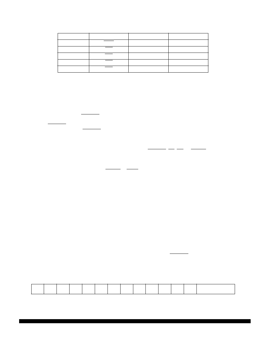
Table 22 CSPAR1 Pin Assignments
CSPAR1 Field
Chip-Select Signal
Alternate Signal
Discrete Output
CS10PA[1:0]
CS10
ADDR23
ECLK
CS9PA[1:0]
CS9
ADDR22
PC6
CS8PA[1:0]
CS8
ADDR21
PC5
CS7PA[1:0]
CS7
ADDR20
PC4
CS6PA[1:0]
CS6
ADDR19
PC3
CSBARBT — Chip-Select Base Address Register Boot ROM
$YFFA48
15
14
13
12
11
10
9
8
7
6
5
4
3
2
1
0
ADDR
23
ADDR
22
ADDR
21
ADDR
20
ADDR
19
ADDR
18
ADDR
17
ADDR
16
ADDR
15
ADDR
14
ADDR
13
ADDR
12
ADDR
11
BLKSZ[2:0]
RESET:
0
1
F
re
e
sc
a
le
S
e
m
ic
o
n
d
u
c
to
r,
I
Freescale Semiconductor, Inc.
For More Information On This Product,
Go to: www.freescale.com
n
c
..
.
相關(guān)PDF資料 |
PDF描述 |
|---|---|
| MC68EN360CRC25 | 32-BIT, 25 MHz, RISC MICROCONTROLLER, CPGA241 |
| MC68F333FE | 32-BIT, FLASH, 16.78 MHz, MICROCONTROLLER, CQFP160 |
| MC68F333FC | 32-BIT, FLASH, 16.78 MHz, MICROCONTROLLER, PQFP160 |
| MC68HC000L12F | 16-BIT, 16.67 MHz, MICROPROCESSOR, CDIP64 |
| MC68HC000L16 | 16-BIT, 16.67 MHz, MICROPROCESSOR, CDIP64 |
相關(guān)代理商/技術(shù)參數(shù) |
參數(shù)描述 |
|---|---|
| MC68CK338CPV14B1 | 制造商:FREESCALE 制造商全稱:Freescale Semiconductor, Inc 功能描述:32-Bit Modular Microcontroller |
| MC68CM16Z1 | 制造商:FREESCALE 制造商全稱:Freescale Semiconductor, Inc 功能描述:M68HC16Z Series |
| MC68CM16Z1CFC16 | 制造商:FREESCALE 制造商全稱:Freescale Semiconductor, Inc 功能描述:M68HC16Z Series |
| MC68CM16Z1CPV16 | 制造商:FREESCALE 制造商全稱:Freescale Semiconductor, Inc 功能描述:M68HC16Z Series |
| MC68E360VR25VLR2 | 功能描述:微處理器 - MPU QUICC ETHRN RoHS:否 制造商:Atmel 處理器系列:SAMA5D31 核心:ARM Cortex A5 數(shù)據(jù)總線寬度:32 bit 最大時(shí)鐘頻率:536 MHz 程序存儲(chǔ)器大小:32 KB 數(shù)據(jù) RAM 大小:128 KB 接口類型:CAN, Ethernet, LIN, SPI,TWI, UART, USB 工作電源電壓:1.8 V to 3.3 V 最大工作溫度:+ 85 C 安裝風(fēng)格:SMD/SMT 封裝 / 箱體:FBGA-324 |
發(fā)布緊急采購(gòu),3分鐘左右您將得到回復(fù)。