- 您現(xiàn)在的位置:買賣IC網(wǎng) > PDF目錄69025 > MC68CK338CPV14 (FREESCALE SEMICONDUCTOR INC) 32-BIT, 14.4 MHz, MICROCONTROLLER, PQFP144 PDF資料下載
參數(shù)資料
| 型號(hào): | MC68CK338CPV14 |
| 廠商: | FREESCALE SEMICONDUCTOR INC |
| 元件分類: | 微控制器/微處理器 |
| 英文描述: | 32-BIT, 14.4 MHz, MICROCONTROLLER, PQFP144 |
| 封裝: | PLASTIC, TQFP-144 |
| 文件頁(yè)數(shù): | 59/133頁(yè) |
| 文件大小: | 944K |
| 代理商: | MC68CK338CPV14 |
第1頁(yè)第2頁(yè)第3頁(yè)第4頁(yè)第5頁(yè)第6頁(yè)第7頁(yè)第8頁(yè)第9頁(yè)第10頁(yè)第11頁(yè)第12頁(yè)第13頁(yè)第14頁(yè)第15頁(yè)第16頁(yè)第17頁(yè)第18頁(yè)第19頁(yè)第20頁(yè)第21頁(yè)第22頁(yè)第23頁(yè)第24頁(yè)第25頁(yè)第26頁(yè)第27頁(yè)第28頁(yè)第29頁(yè)第30頁(yè)第31頁(yè)第32頁(yè)第33頁(yè)第34頁(yè)第35頁(yè)第36頁(yè)第37頁(yè)第38頁(yè)第39頁(yè)第40頁(yè)第41頁(yè)第42頁(yè)第43頁(yè)第44頁(yè)第45頁(yè)第46頁(yè)第47頁(yè)第48頁(yè)第49頁(yè)第50頁(yè)第51頁(yè)第52頁(yè)第53頁(yè)第54頁(yè)第55頁(yè)第56頁(yè)第57頁(yè)第58頁(yè)當(dāng)前第59頁(yè)第60頁(yè)第61頁(yè)第62頁(yè)第63頁(yè)第64頁(yè)第65頁(yè)第66頁(yè)第67頁(yè)第68頁(yè)第69頁(yè)第70頁(yè)第71頁(yè)第72頁(yè)第73頁(yè)第74頁(yè)第75頁(yè)第76頁(yè)第77頁(yè)第78頁(yè)第79頁(yè)第80頁(yè)第81頁(yè)第82頁(yè)第83頁(yè)第84頁(yè)第85頁(yè)第86頁(yè)第87頁(yè)第88頁(yè)第89頁(yè)第90頁(yè)第91頁(yè)第92頁(yè)第93頁(yè)第94頁(yè)第95頁(yè)第96頁(yè)第97頁(yè)第98頁(yè)第99頁(yè)第100頁(yè)第101頁(yè)第102頁(yè)第103頁(yè)第104頁(yè)第105頁(yè)第106頁(yè)第107頁(yè)第108頁(yè)第109頁(yè)第110頁(yè)第111頁(yè)第112頁(yè)第113頁(yè)第114頁(yè)第115頁(yè)第116頁(yè)第117頁(yè)第118頁(yè)第119頁(yè)第120頁(yè)第121頁(yè)第122頁(yè)第123頁(yè)第124頁(yè)第125頁(yè)第126頁(yè)第127頁(yè)第128頁(yè)第129頁(yè)第130頁(yè)第131頁(yè)第132頁(yè)第133頁(yè)
MC68CK338
MOTOROLA
MC68CK338TS/D
31
When a memory access occurs, chip-select logic compares address space type, address, type of ac-
cess, transfer size, and interrupt priority (in the case of interrupt acknowledge) to parameters stored in
chip-select registers. If all parameters match, the appropriate chip-select signal is asserted. Select sig-
nals are active low. If a chip-select function is given the same address as a microcontroller module or
an internal memory array, an access to that address goes to the module or array, and the chip-select
signal is not asserted. The external address and data buses do not reflect the internal access.
All chip-select circuits except CSBOOT are disabled out of reset. Chip-select option registers must not
be written until base addresses have been written to the proper base address registers. Alternate func-
tions for chip-select pins are enabled if appropriate data bus pins are held low at the release of RESET.
Table 17 lists allocation of chip-selects and discrete outputs on the pins of the MCU.
3.6.1 Chip-Select Registers
Each chip-select pin can have one or more functions. Chip-select pin assignment registers CSPAR[0:1]
determine functions of the pins. Pin assignment registers also determine port size for dynamic bus al-
location. A pin data register (PORTC) latches data for chip-select pins that are used for discrete output.
Blocks of addresses are assigned to each chip-select function. Block sizes of two Kbytes to one Mbyte
can be selected by writing values to the appropriate base address registers CSBARBT and CS-
BAR[0:10]. Multiple chip-selects assigned to the same block of addresses must have the same number
of wait states.
Chip-select option registers CSORBT and CSOR[0:10] determine timing of and conditions for assertion
of chip-select signals. Eight parameters, including operating mode, access size, synchronization, and
wait state insertion can be specified.
Initialization software usually resides in a peripheral memory device controlled by the chip-select cir-
cuits. CSBOOT and registers CSORBT and CSBARBT are provided to support bootstrap operation.
3.6.2 Pin Assignment Registers
The pin assignment registers contain twelve 2-bit fields that determine functions of the chip-select pins.
Each pin has two or three possible functions, as shown in Table 18.
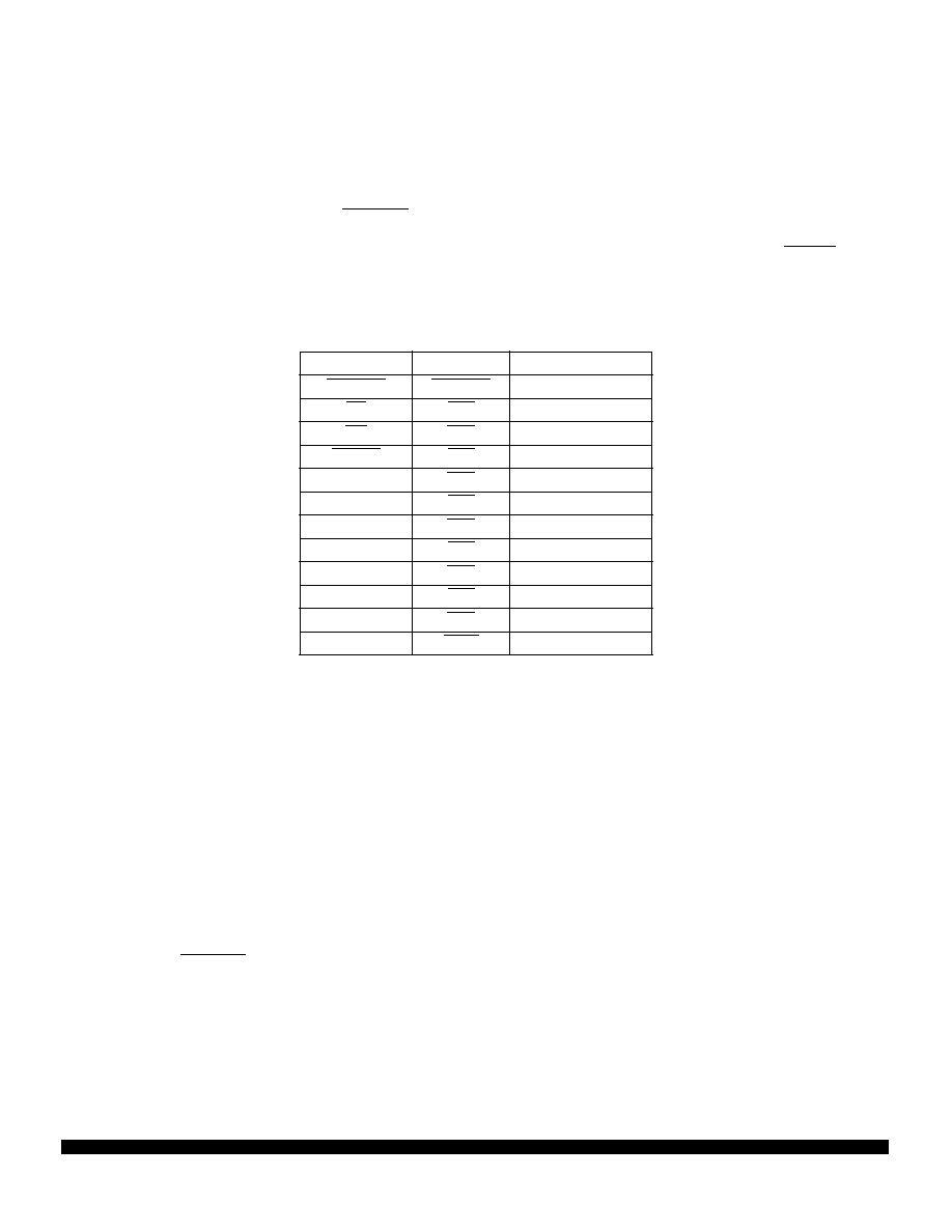
Table 17 Chip-Select and Discrete Output Allocation
Pin
Chip-Select
Discrete Outputs
CSBOOT
—
BR
CS0
—
BG
CS1
—
BGACK
CS2
—
FC0
CS3
PC0
FC1
CS4
PC1
FC2
CS5
PC2
ADDR19
CS6
PC3
ADDR20
CS7
PC4
ADDR21
CS8
PC5
ADDR22
CS9
PC6
ADDR23
CS10
—
F
re
e
sc
a
le
S
e
m
ic
o
n
d
u
c
to
r,
I
Freescale Semiconductor, Inc.
For More Information On This Product,
Go to: www.freescale.com
n
c
..
.
相關(guān)PDF資料 |
PDF描述 |
|---|---|
| MC68EN360CRC25 | 32-BIT, 25 MHz, RISC MICROCONTROLLER, CPGA241 |
| MC68F333FE | 32-BIT, FLASH, 16.78 MHz, MICROCONTROLLER, CQFP160 |
| MC68F333FC | 32-BIT, FLASH, 16.78 MHz, MICROCONTROLLER, PQFP160 |
| MC68HC000L12F | 16-BIT, 16.67 MHz, MICROPROCESSOR, CDIP64 |
| MC68HC000L16 | 16-BIT, 16.67 MHz, MICROPROCESSOR, CDIP64 |
相關(guān)代理商/技術(shù)參數(shù) |
參數(shù)描述 |
|---|---|
| MC68CK338CPV14B1 | 制造商:FREESCALE 制造商全稱:Freescale Semiconductor, Inc 功能描述:32-Bit Modular Microcontroller |
| MC68CM16Z1 | 制造商:FREESCALE 制造商全稱:Freescale Semiconductor, Inc 功能描述:M68HC16Z Series |
| MC68CM16Z1CFC16 | 制造商:FREESCALE 制造商全稱:Freescale Semiconductor, Inc 功能描述:M68HC16Z Series |
| MC68CM16Z1CPV16 | 制造商:FREESCALE 制造商全稱:Freescale Semiconductor, Inc 功能描述:M68HC16Z Series |
| MC68E360VR25VLR2 | 功能描述:微處理器 - MPU QUICC ETHRN RoHS:否 制造商:Atmel 處理器系列:SAMA5D31 核心:ARM Cortex A5 數(shù)據(jù)總線寬度:32 bit 最大時(shí)鐘頻率:536 MHz 程序存儲(chǔ)器大小:32 KB 數(shù)據(jù) RAM 大小:128 KB 接口類型:CAN, Ethernet, LIN, SPI,TWI, UART, USB 工作電源電壓:1.8 V to 3.3 V 最大工作溫度:+ 85 C 安裝風(fēng)格:SMD/SMT 封裝 / 箱體:FBGA-324 |
發(fā)布緊急采購(gòu),3分鐘左右您將得到回復(fù)。