- 您現(xiàn)在的位置:買賣IC網(wǎng) > PDF目錄370961 > M44C090-H (ATMEL CORP) Low-Current Microcontroller for Wireless Communication PDF資料下載
參數(shù)資料
| 型號(hào): | M44C090-H |
| 廠商: | ATMEL CORP |
| 元件分類: | 微控制器/微處理器 |
| 英文描述: | Low-Current Microcontroller for Wireless Communication |
| 中文描述: | 4-BIT, MROM, 4 MHz, MICROCONTROLLER, PDSO20 |
| 封裝: | SSO-20 |
| 文件頁數(shù): | 38/63頁 |
| 文件大?。?/td> | 503K |
| 代理商: | M44C090-H |
第1頁第2頁第3頁第4頁第5頁第6頁第7頁第8頁第9頁第10頁第11頁第12頁第13頁第14頁第15頁第16頁第17頁第18頁第19頁第20頁第21頁第22頁第23頁第24頁第25頁第26頁第27頁第28頁第29頁第30頁第31頁第32頁第33頁第34頁第35頁第36頁第37頁當(dāng)前第38頁第39頁第40頁第41頁第42頁第43頁第44頁第45頁第46頁第47頁第48頁第49頁第50頁第51頁第52頁第53頁第54頁第55頁第56頁第57頁第58頁第59頁第60頁第61頁第62頁第63頁
M44C890
M44C090
Rev.A4, 14-Dec-01
38 (63)
3.3.3
SSI Features:
Synchronous Serial Interface (SSI)
2 and 3 wire NRZ
2 wire mode (I
2
C compatible)
(additional internal 2 wire link for multi-chip
packaging solutions)
With Timer 2:
Biphase modulation
Manchester modulation
pulse-width demodulation
Burst modulation
SSI Peripheral Configuration
The synchronous serial interface (SSI) can be used either
for serial communication with external devices such as
EEPROMs, shift registers, display drivers, other
microcontrollers, or as a means for generating and
capturing on-chip serial streams of data. External data
communication takes place via the Port 4 (BP4)
multi-functional port which can be software configured
by writing the appropriate control word into the P4CR
register. The SSI can be configured in any one of the
following ways:
a)
communication with one data terminal and one shift
clock. The SSI uses the Port BP43 as a bidirectional serial
data line (SD) and BP40 as shift clock line (SC).
2-wire external interface for bidirectional data
b)
and output of serial data, with a serial input data terminal
3-wire external interface for simultaneous input
(SI), a serial output data terminal (SO) and a shift clock
(SC). The SSI uses BP40 as shift clock (SC), while the
serial data input (SI) is applied to BP43 (configured in
P4CR as input!). Serial output data (SO) in this case is
passed through to BP42 (configured in P4CR to T2O) via
the Timer 2 output stage (T2M2 configured in mode 6).
c)
together with Timer 2 is capable of performing a variety
of data modulation and functions (see Timer Section).
The modulating data is converted by the SSI into a
continuous serial stream of data which is in turn
modulated in one of the timer functional blocks.
Timer/SSI combined modes
–
the SSI used
d)
as an interchip data interface for use in single package
multi
–
chip modules or hybrids. For such applications, the
SSI is provided with two dedicated pads (MCL_SD and
MCL_SC) which act as a two-wire chip-to-chip link. The
MCL can be activated by the MCL control bit. Should
these MCL pads be used by the SSI, the standard SD and
SC pins are not required and the corresponding Port 4
ports are available as conventional data ports.
General SSI Operation
Multi-chip link (MCL)
–
the SSI can also be used
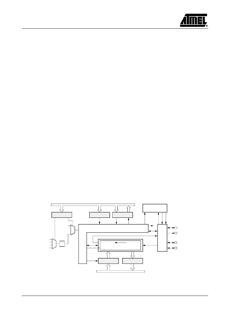
The SSI is comprised essentially of an 8-bit shift register
with two associated 8-bit buffers
–
the receive buffer
(SRB) for capturing the incoming serial data and a trans-
mit buffer (STB) for intermediate storage of data to be
serially output. Both buffers are directly accessable by
software. Transferring the parallel buffer data into and out
of the shift register is controlled automatically by the SSI
control, so that both single byte transfers or continuous bit
streams can be supported.
14103
8-bit Shift Register
MSB
LSB
Shift_CL
SO
SIC1
SIC2
SISC
SC
Control
STB
SRB
SI
Timer 2
Output
INT3
SC
I/O
–
bus
I/O-bus
SSI-Control
TOG2
POUT
T1OUT
SYSCL
SO
SI
MCL_SC
SD
MCL_SD
Transmit
Buffer
Receive
Buffer
SCI
/2
Figure 43. Block diagram of the synchronous serial interface
相關(guān)PDF資料 |
PDF描述 |
|---|---|
| M44C890 | Low-Current Microcontroller for Wireless Communication |
| M44C890-H | Low-Current Microcontroller for Wireless Communication |
| M4N25 | 6-Pin DIP Optoisolators Transistor Output |
| M4N26 | 6-Pin DIP Optoisolators Transistor Output |
| M4N37 | Header, Vertical Friction Lock; No. of Contacts:3; Pitch Spacing:2.54mm; No. of Rows:1; Gender:Header; Series:6410; Body Material:PA Polyamide (Nylon); Current Rating:4A; Voltage Rating:250V RoHS Compliant: Yes |
相關(guān)代理商/技術(shù)參數(shù) |
參數(shù)描述 |
|---|---|
| M44C890 | 制造商:ATMEL 制造商全稱:ATMEL Corporation 功能描述:Low-Current Microcontroller for Wireless Communication |
| M44C890-H | 制造商:ATMEL 制造商全稱:ATMEL Corporation 功能描述:Low-Current Microcontroller for Wireless Communication |
| M44S05K4F1 | 功能描述:汽車連接器 MX44 Terminals RoHS:否 制造商:Amphenol SINE Systems 產(chǎn)品:Contacts 系列:ATP 位置數(shù)量: 型式:Female 安裝風(fēng)格: 端接類型: 觸點(diǎn)電鍍:Nickel |
| M44T332538880MHZ | 制造商:MEC 功能描述: |
| M44T3338880MHZ | 制造商:MEC 功能描述: |
發(fā)布緊急采購,3分鐘左右您將得到回復(fù)。