- 您現(xiàn)在的位置:買賣IC網(wǎng) > PDF目錄377815 > M29W004T (意法半導(dǎo)體) 4Mbit (512Kb x8, Boot Block) Low Voltage Single Supply Flash Memory(4Mb閃速存儲器) PDF資料下載
參數(shù)資料
| 型號: | M29W004T |
| 廠商: | 意法半導(dǎo)體 |
| 英文描述: | 4Mbit (512Kb x8, Boot Block) Low Voltage Single Supply Flash Memory(4Mb閃速存儲器) |
| 中文描述: | 的4Mb(512KB的× 8,引導(dǎo)塊)低電壓單電源閃存(4Mb的閃速存儲器) |
| 文件頁數(shù): | 17/30頁 |
| 文件大小: | 199K |
| 代理商: | M29W004T |
第1頁第2頁第3頁第4頁第5頁第6頁第7頁第8頁第9頁第10頁第11頁第12頁第13頁第14頁第15頁第16頁當(dāng)前第17頁第18頁第19頁第20頁第21頁第22頁第23頁第24頁第25頁第26頁第27頁第28頁第29頁第30頁
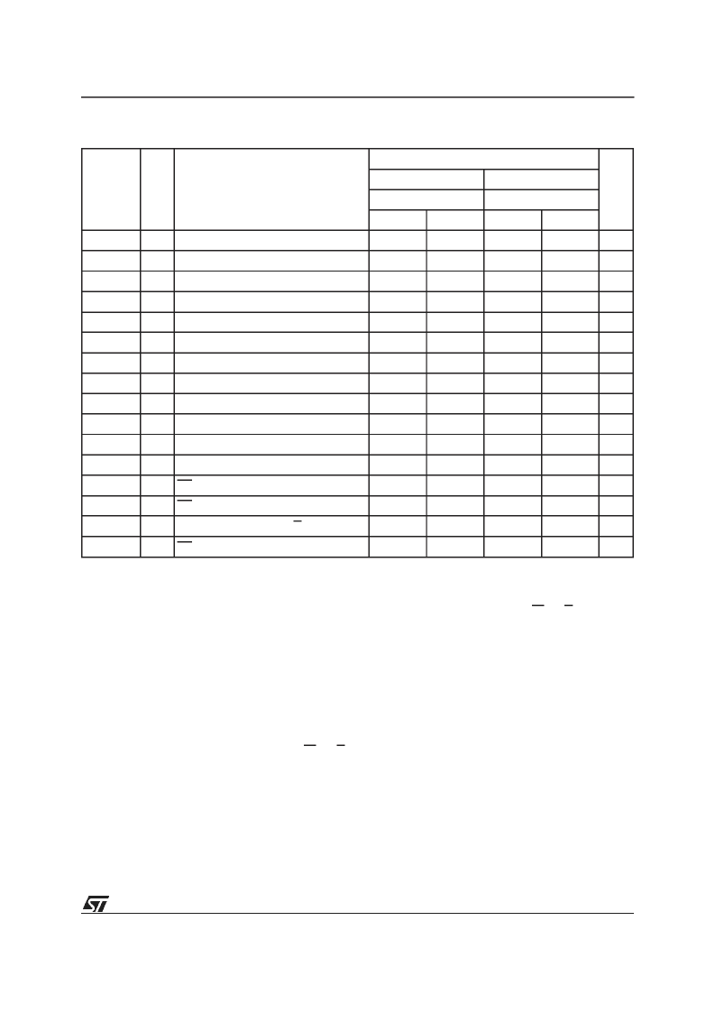
Symbol
Alt
Parameter
M29W004T / M29W004B
Unit
-120
-150
V
CC
= 2.7V to 3.6V
V
CC
= 2.7V to 3.6V
Min
Max
Min
Max
t
AVAV
t
WC
Address Validto Next Address Valid
120
150
ns
t
ELWL
t
CS
Chip Enable Low to Write Enable Low
0
0
ns
t
WLWH
t
WP
Write Enable Low to Write Enable High
50
65
ns
t
DVWH
t
DS
Input Valid to Write Enable High
50
65
ns
t
WHDX
t
DH
Write Enable High to Input Transition
0
0
ns
t
WHEH
t
CH
Write Enable High to Chip Enable High
0
0
ns
t
WHWL
t
WPH
Write Enable High to Write Enable Low
30
35
ns
t
AVWL
t
AS
Address Valid to Write Enable Low
0
0
ns
t
WLAX
t
AH
Write Enable Low to Address Transition
50
65
ns
t
GHWL
Output Enable High to Write Enable Low
0
0
ns
t
VCHEL
t
VCS
V
CC
High to Chip Enable Low
50
50
μ
s
t
WHGL
t
OEH
Write Enable High to Output Enable Low
0
0
ns
t
PHPHH
(1,2)
t
VIDR
RP Rise Timeto V
ID
500
500
ns
t
PLPX
t
RP
RP Pulse Width
500
500
ns
t
WHRL
(1)
t
BUSY
Program Erase Valid to RB Delay
90
90
ns
t
PHWL(1)
t
RSP
RP High to Write Enable Low
4
4
μ
s
Notes:
1. Sample only, not 100% tested.
2. This timing is for Temporary Block Unprotectionoperation.
Table15B. Write AC Characteristics,Write Enable Controlled
(T
A
= 0 to 70
°
C, –20 to 85
°
C or–40 to 85
°
C)
after the sixth rising edge of W or E output the
status register status bits.
DuringtheexecutionoftheerasebytheP/E.C.,the
memory accepts onlythe Erase Suspend ES and
Read/Reset RD instructions.Data Polling bit DQ7
returns ’0’ while the erasure is in progress and ’1’
when it has completed. The Toggle bit DQ2 and
DQ6 toggleduring the erase operation.They stop
when erase is completed. After completion the
StatusRegisterbit DQ5returns’1’if therehasbeen
an erase failure. In such a situation,the Toggle bit
DQ2 can be used to determine which block is not
correctly erased. In the case of erase failure, a
Read/ResetRD instructionis necessaryin orderto
reset the P/E.C.
ChipErase(CE)Instruction.
Thisinstructionuses
six write cycles. The Erase Set-up command 80h
is written to address5555h on the third cycle after
the two Coded cycles. The Chip Erase Confirm
command10h is similarly writtenon the sixthcycle
after another two Coded cycles. If the second
command given is not an erase confirm or if the
Codedcyclesarewrong,the instructionabortsand
thedeviceisresetto ReadArray.Itisnotnecessary
toprogramthearraywith00hfirstastheP/E.C.will
automaticallydo thisbeforeerasingit toFFh.Read
operations after the sixth rising edge of W or E
output the Status Register bits. During the execu-
tionof theerasebytheP/E.C.,DataPollingbitDQ7
returns ’0’, then ’1’ on completion. The Togglebits
DQ2 and DQ6 toggle during erase operation and
17/30
M29W004T M29W004B
相關(guān)PDF資料 |
PDF描述 |
|---|---|
| M29W008AB | 8Mbit(1Mbx8, Boot Block) Low Voltage Single Supply Flash Memory(8Mb閃速存儲器) |
| M29W008AT | 8Mbit(1Mbx8, Boot Block) Low Voltage Single Supply Flash Memory(8Mb閃速存儲器) |
| M29W008B | 8 Mbit (1Mb x8, Boot Block) Low Voltage Single Supply Flash Memory(8 M位 (1Mb x8,導(dǎo)入塊)低壓單電源閃速存儲器) |
| M29W010B45K6F | 1 Mbit 128Kb x8, Uniform Block Low Voltage Single Supply Flash Memory |
| M29W010B45N1 | 1 Mbit 128Kb x8, Uniform Block Low Voltage Single Supply Flash Memory |
相關(guān)代理商/技術(shù)參數(shù) |
參數(shù)描述 |
|---|---|
| M29W004T-100N1TR | 制造商:STMICROELECTRONICS 制造商全稱:STMicroelectronics 功能描述:4 Mbit 512Kb x8, Boot Block Low Voltage Single Supply Flash Memory |
| M29W004T-100N5TR | 制造商:STMICROELECTRONICS 制造商全稱:STMicroelectronics 功能描述:4 Mbit 512Kb x8, Boot Block Low Voltage Single Supply Flash Memory |
| M29W004T-100N6TR | 制造商:STMICROELECTRONICS 制造商全稱:STMicroelectronics 功能描述:4 Mbit 512Kb x8, Boot Block Low Voltage Single Supply Flash Memory |
| M29W004T-120N1TR | 制造商:STMICROELECTRONICS 制造商全稱:STMicroelectronics 功能描述:4 Mbit 512Kb x8, Boot Block Low Voltage Single Supply Flash Memory |
| M29W004T-120N5TR | 制造商:STMICROELECTRONICS 制造商全稱:STMicroelectronics 功能描述:4 Mbit 512Kb x8, Boot Block Low Voltage Single Supply Flash Memory |
發(fā)布緊急采購,3分鐘左右您將得到回復(fù)。