- 您現(xiàn)在的位置:買賣IC網(wǎng) > PDF目錄377624 > LF3370 (Logic Devices Incorporated) High-Definition Video Format Converter(高清晰度視頻格式轉換器) PDF資料下載
參數(shù)資料
| 型號: | LF3370 |
| 廠商: | Logic Devices Incorporated |
| 英文描述: | High-Definition Video Format Converter(高清晰度視頻格式轉換器) |
| 中文描述: | 高清晰度視頻格式轉換器(高清晰度視頻格式轉換器) |
| 文件頁數(shù): | 13/22頁 |
| 文件大?。?/td> | 256K |
| 代理商: | LF3370 |
DEVICES INCORPORATED
Video Imaging Products
13
LF3370
High-Definition Video Format Converter
08/21/2000–LDS.3370-E
that latches the HIGH to LOW transition
of LD. The next value(s) loaded into the
interface are the data value(s) which will
be stored in the bank or register defined
by the address value. When loading
coefficient banks, the interface will expect
ten values to be loaded into the device
after the address value. The ten values are
coefficients 0 through 8 and the Keyscale
coefficient. When loading Configuration
or Bias Registers, the interface will expect
one value after the address value. When
loading RSL registers, the interface will
expect four values after the address value.
When loading gamma look-up tables, the
interface will expect 1024 values after the
address value. When loading HBLANK
flag counts, the interface will expect 2
values after the address value.
The coefficient banks, configuration
registers, RSL registers, etc., are not
loaded with data until all data values for
the specified address are loaded into the
LF Interface. In other words, the coeffi-
cient banks are not written until all ten
coefficients have been loaded into the LF
DESCRIPTION
ADDRESS RANGE (HEX)
Coefficient Registers
0000 - 0003
Configuration Registers
0200 - 020A
Look-Up Table - Channel ‘A’
0300
Look-Up Table - Channel ‘B’
0400
Look-Up Table - Channel ‘C’
0500
Input Bias Registers - Channel ‘A’
0600 - 0603
Input Bias Registers - Channel ‘B’
0700 - 0703
Input Bias Registers - Channel ‘C’
0800 - 0803
Output Bias Registers - Channel ‘A’
0900 - 0903
Output Bias Registers - Channel ‘B’
0A00 - 0A03
Output Bias Registers - Channel ‘C’
0B00 - 0B03
HF0 Count Value
0C00
HF1 Count Value
0D00
Matrix Mult. RSL Registers - Channel ‘A’
0E00 - 0E03
Matrix Mult. RSL Registers - Channel ‘B’
0F00 - 0F03
Matrix Mult. RSL Registers - Channel ‘C’
1000 - 1003
Key Scaler RSL Registers
1100 - 1103
Half-Band Filter RSL Registers - Channel ‘B’
1200 - 1203
Half-Band Filter RSL Registers - Channel ‘C’
1300 - 1303
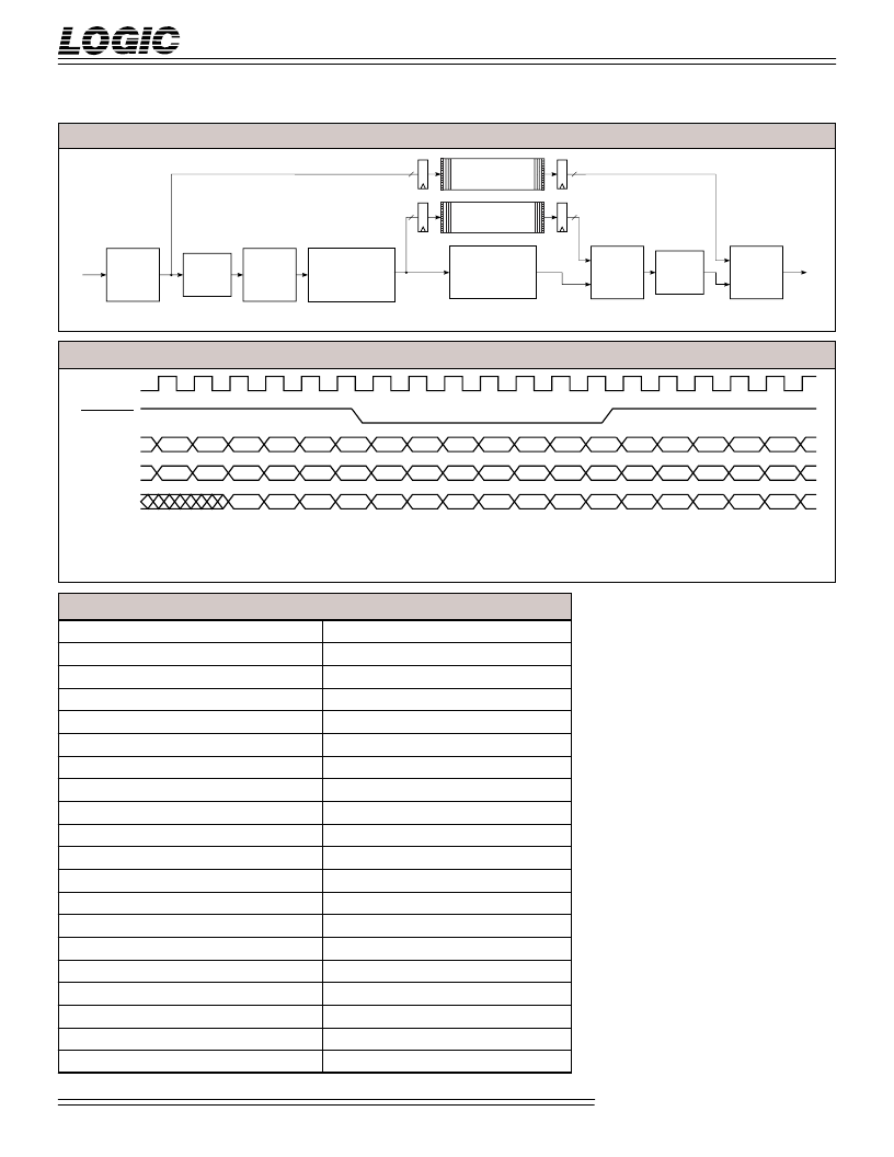
T
ABLE
4.
C
ONFIGURATION
/C
ONTROL
R
EGISTERS
A
DDRESSING
S
UMMARY
F
IGURE
15. B
YPASS
B
LOCK
D
IAGRAM
VBYPASS DELAY
(127 x 13-Bit )
HALF-BAND
FILTER
SECTION
MATRIX MULTIPLIER
and KEY SCALER
SECTION
LUT
SECTION
OUTPUT
BIAS
SECTION
VARIABLE LENGTH
(127 x 13-Bit )
INPUT
BIAS
SECTION
13
INPUT
DEMUX
SECTION
13
OUTPUT
MUX
SECTION
13
LUT
SECTION
A,
B,
C,
D
W,
X,
Y,
Z
13
In this example, the Matrix-Multipler/Key Scaler Section feeds the Half-Band Filter Section. This arrangement is reversible.
F
IGURE
16.
C
ORE
B
YPASS
CLK
In this example, the Output Multiplexer is in a mode where the delay through the section is 2 CLK cycles. Only one channel is shown in this example,
however, the other three channels behave in the same manner. The example assumes that the bypass RAM length is set to the length of the core data path.
W1: Bypass data is output to the output port and replaces core data.
W2: Core data is output to the output port and replaces bypass data.
Core Data
D
0
D
1
D
2
D
3
D
4
D
5
D
6
D
7
D
8
D
9
D
10
D
11
D
12
*
Output*
D
13
D
14
D
15
D
16
D
17
DATAPASS
B
0
B
1
B
2
B
3
B
4
B
5
B
6
B
7
B
8
B
9
B
10
B
11
B
12
B
13
B
14
B
15
B
16
B
17
D
0
D
1
D
2
D
3
D
4
D
5
B
6
B
7
B
8
B
9
B
10
B
11
B
12
D
13
D
14
D
15
Bypass Data
W1
W2
相關PDF資料 |
PDF描述 |
|---|---|
| LF39J8 | DIODE ZENER TRIPLE ISOLATED 200mW 8.2Vz 20mA-Izt 0.05 3uA-Ir 6.5 SOT-363 3K/REEL |
| LF43881JC40 | 8 x 8-bit Digital Filter |
| LF43881 | 8 x 8-bit Digital Filter |
| LF48212QC20 | 12 x 12-bit Alpha Mixer |
| LF48212QC25 | 12 x 12-bit Alpha Mixer |
相關代理商/技術參數(shù) |
參數(shù)描述 |
|---|---|
| LF3370QC12 | 制造商:LOGIC 制造商全稱:LOGIC 功能描述:High-Definition Video Format Converter |
| LF33AB | 制造商:STMICROELECTRONICS 制造商全稱:STMicroelectronics 功能描述:Very low drop voltage regulators with inhibit |
| LF33ABDT | 功能描述:低壓差穩(wěn)壓器 - LDO 3.3V 0.5A Positive RoHS:否 制造商:Texas Instruments 最大輸入電壓:36 V 輸出電壓:1.4 V to 20.5 V 回動電壓(最大值):307 mV 輸出電流:1 A 負載調節(jié):0.3 % 輸出端數(shù)量: 輸出類型:Fixed 最大工作溫度:+ 125 C 安裝風格:SMD/SMT 封裝 / 箱體:VQFN-20 |
| LF33ABDT-TR | 功能描述:低壓差穩(wěn)壓器 - LDO 3.3V 0.5A Positive RoHS:否 制造商:Texas Instruments 最大輸入電壓:36 V 輸出電壓:1.4 V to 20.5 V 回動電壓(最大值):307 mV 輸出電流:1 A 負載調節(jié):0.3 % 輸出端數(shù)量: 輸出類型:Fixed 最大工作溫度:+ 125 C 安裝風格:SMD/SMT 封裝 / 箱體:VQFN-20 |
| LF33ABP | 功能描述:低壓差穩(wěn)壓器 - LDO 3.3V 0.5A Positive RoHS:否 制造商:Texas Instruments 最大輸入電壓:36 V 輸出電壓:1.4 V to 20.5 V 回動電壓(最大值):307 mV 輸出電流:1 A 負載調節(jié):0.3 % 輸出端數(shù)量: 輸出類型:Fixed 最大工作溫度:+ 125 C 安裝風格:SMD/SMT 封裝 / 箱體:VQFN-20 |
發(fā)布緊急采購,3分鐘左右您將得到回復。