- 您現(xiàn)在的位置:買賣IC網(wǎng) > PDF目錄67683 > IBM25PPC750GLECR5HA3T 32-BIT, 1000 MHz, RISC PROCESSOR, CBGA292 PDF資料下載
參數(shù)資料
| 型號(hào): | IBM25PPC750GLECR5HA3T |
| 元件分類: | 微控制器/微處理器 |
| 英文描述: | 32-BIT, 1000 MHz, RISC PROCESSOR, CBGA292 |
| 封裝: | 21X 21 MM, 1 MM PITCH, CERAMIC, BGA-292 |
| 文件頁(yè)數(shù): | 57/76頁(yè) |
| 文件大小: | 1031K |
| 代理商: | IBM25PPC750GLECR5HA3T |
第1頁(yè)第2頁(yè)第3頁(yè)第4頁(yè)第5頁(yè)第6頁(yè)第7頁(yè)第8頁(yè)第9頁(yè)第10頁(yè)第11頁(yè)第12頁(yè)第13頁(yè)第14頁(yè)第15頁(yè)第16頁(yè)第17頁(yè)第18頁(yè)第19頁(yè)第20頁(yè)第21頁(yè)第22頁(yè)第23頁(yè)第24頁(yè)第25頁(yè)第26頁(yè)第27頁(yè)第28頁(yè)第29頁(yè)第30頁(yè)第31頁(yè)第32頁(yè)第33頁(yè)第34頁(yè)第35頁(yè)第36頁(yè)第37頁(yè)第38頁(yè)第39頁(yè)第40頁(yè)第41頁(yè)第42頁(yè)第43頁(yè)第44頁(yè)第45頁(yè)第46頁(yè)第47頁(yè)第48頁(yè)第49頁(yè)第50頁(yè)第51頁(yè)第52頁(yè)第53頁(yè)第54頁(yè)第55頁(yè)第56頁(yè)當(dāng)前第57頁(yè)第58頁(yè)第59頁(yè)第60頁(yè)第61頁(yè)第62頁(yè)第63頁(yè)第64頁(yè)第65頁(yè)第66頁(yè)第67頁(yè)第68頁(yè)第69頁(yè)第70頁(yè)第71頁(yè)第72頁(yè)第73頁(yè)第74頁(yè)第75頁(yè)第76頁(yè)
Datasheet
DD1.X
IBM PowerPC 750GL RISC Microprocessor
Preliminary
System Design Information
Page 60 of 74
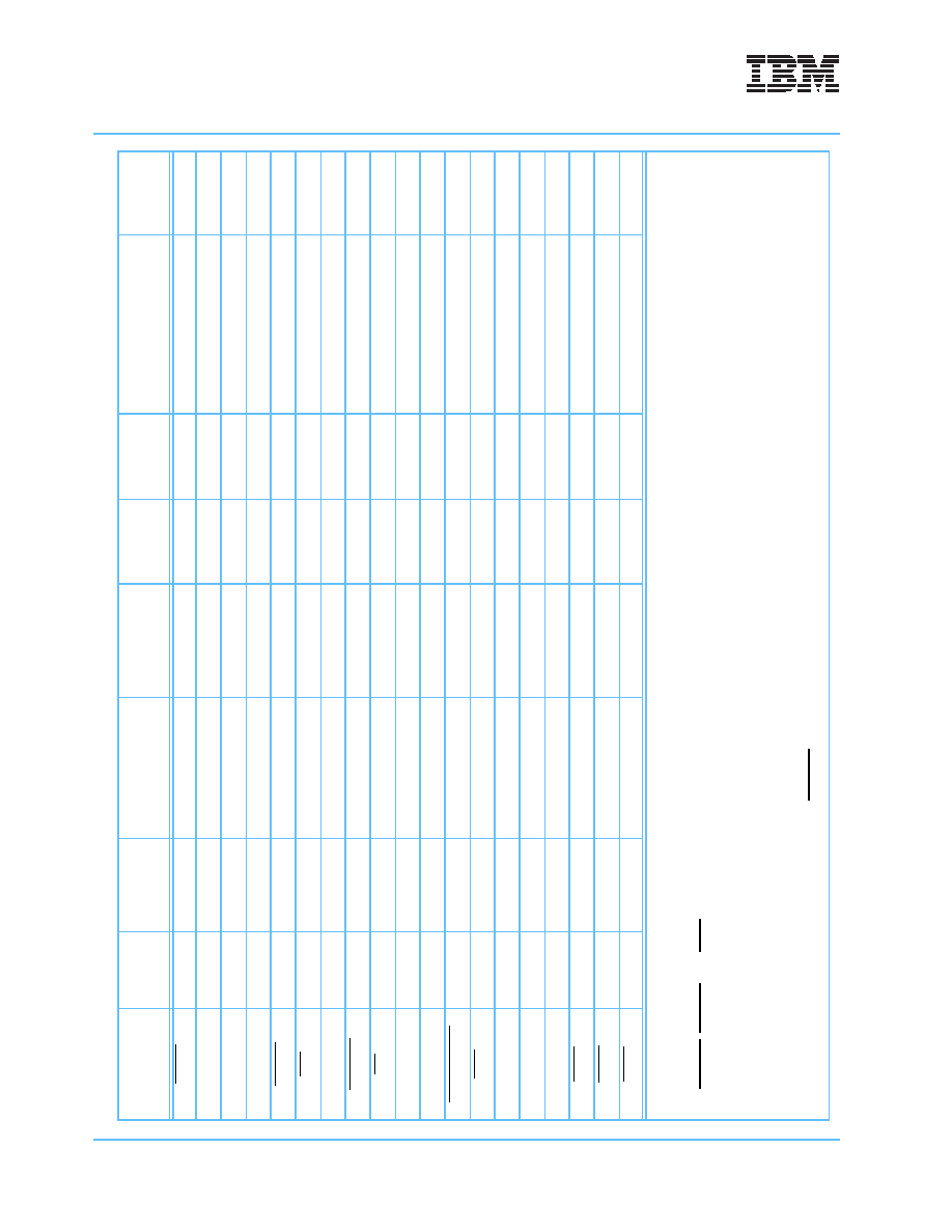
750GL_ds_body.fm.1.2
March 13, 2006
DB
W
O
Low
Input
Mode
Select
/C
ont
rol
K
eeper
4,
DH
[0
:31]
High
Input
/O
u
tput
Da
ta
Bus
K
eeper
3,
DL[
0
:31]
High
Input
/O
u
tput
Da
ta
Bus
K
eeper
3,
DP[
0
:7
]
High
Input
/O
u
tput
—
DRTRY
Low
Input
—
K
eeper
4,
GB
L
Low
Input
/O
u
tput
T
rans
fe
rAt
tr
ib
u
tes
K
eeper
3,
G
N
D
—
P
owe
rS
upply
HRE
S
E
T
Low
Input
In
te
rrupt
/R
es
et
s
K
eeper
Ac
ti
ve
driver
2,
3,
4,
INT
Low
Input
In
te
rrupt
/R
es
et
s
K
eeper
Ac
ti
ve
driver
or
pull
u
p
,4,
L
1_T
S
T
C
L
K
High
Input
Mode
Select
/C
ont
rol
N
ot
en
abl
ed
5
K
Pullup/
pull
dow
n,
as
required
L
2_T
S
T
C
L
K
High
Input
LS
SD
Not
en
abl
ed
5
K
Pullup
required
t
o
O
V
DD
6
LS
SD_M
O
D
E
Low
Input
LS
SD
Not
en
abl
ed
5
K
Pullup
required
t
o
O
V
DD
MCP
Low
Input
In
te
rrupt
/R
es
et
s
K
eeper
Ac
ti
ve
driver
or
pull
u
p
,4,
OV
DD
—
Powe
rS
upply
PLL_C
F
G
[0
:4
]
High
Input
C
loc
k
Cont
ro
l
K
eeper
A
s
required
P
ullup/
pull
dow
n,
as
required
,4,
P
LL_RNG
[0
:1
]
High
Input
—
K
eeper
A
s
required
P
ullup/
pull
dow
n,
as
required
,4,
QACK
Low
Input
Mode
Select
ont
rol
K
eeper
Mus
tbe
a
c
ti
ve
ly
drive
n
4,
5,
QRE
Q
Low
O
u
tput
S
tat
us/
C
ont
ro
l
K
eeper
Chip
a
c
ti
vely
drive
s
5
RS
RV
Low
O
u
tput
—
K
eeper
No
connect
,4,
T
a
b
le
5
-6
.
In
put/
O
u
tpu
tUs
age
(
C
onti
nue
d)
750G
L
Signal
Nam
e
Act
ive
Level
Input
/
Ou
tp
u
t
Us
age
G
roup
Input
/O
u
tput
wit
h
In
te
rnal
P
u
llup
Resist
ors
Le
vel
P
rot
ec
t
Required
Ext
e
rnal
R
e
si
st
or
Comm
ent
s
N
ot
es
No
te
s:
1.
D
epends
on
the
s
yst
em
design.
T
he
el
e
c
tr
ic
al
char
act
e
rist
ic
s
of
t
he
750G
L
do
not
add
addi
ti
onal
c
onst
raint
s
to
t
he
s
yst
em
des
ign
,so
what
ever
is
d
one
wit
h
t
he
net
w
ill
de
pend
on
t
he
sy
st
e
m
requiremen
ts.
2.
H
R
ES
ET
,S
R
ES
ET
,and
T
R
S
T
are
signals
used
f
o
r
RI
SCW
a
tc
h
to
enab
le
proper
operat
ion
of
the
debuggers.
Lo
gi
c
a
lAN
D
gat
es
should
be
placed
bet
ween
these
s
ignals
an
d
t
he
I
B
M
P
o
werP
C
750G
L
RI
S
C
M
icropr
ocess
o
r(
s
ee
F
igure
5
-6
on
p
age
63).
3.
T
he
750G
L
pr
ovides
pr
ot
ect
ion
f
rom
m
e
ta
-st
abil
it
y
on
input
s
t
h
rough
t
he
use
of
a
“k
eeper”
c
ir
c
uit
on
s
pecif
ic
input
s
(see
Se
c
ti
o
n
5
.8
on
p
age
71
f
o
ra
mor
e
det
ailed
des
crip-
ti
on).
4.
If
a
sys
te
m
design
requires
a
signal
level
t
o
be
maint
a
ined
while
not
being
act
ively
driv
en,
an
ex
te
rnal
resist
or
device
m
ust
be
us
ed
(kee
pers
as
sure
no
met
a
-st
abili
ty
of
input
s
but
do
not
guarant
ee
a
level).
5.
T
he
750G
L
does
not
r
equire
ex
te
rn
al
pullup
s
on
addr
ess
and
dat
a
lines
.
Cont
ro
l
lines
m
u
st
be
t
reat
ed
individually
.
6.
M
ode
Select
/C
on
tr
ol
pi
ns
r
equi
re
t
he
pr
oper
s
tat
e
a
tHRES
E
T
to
c
onf
igure
the
oper
at
ing
mode
of
t
he
proc
essor
(se
e
T
able
5-10,
Sum
m
ary
of
M
ode
S
e
lect
,on
p
age
72).
相關(guān)PDF資料 |
PDF描述 |
|---|---|
| IBM25PPC750GXEAR5H42T | 32-BIT, 933 MHz, RISC PROCESSOR, CBGA292 |
| IBM25PPC750GXEBB6H42T | 32-BIT, 1000 MHz, RISC PROCESSOR, CBGA292 |
| IBM25PPC750GXEBR2H33T | 32-BIT, 800 MHz, RISC PROCESSOR, CBGA292 |
| IBM25PPC750GXECB5H43T | 32-BIT, 933 MHz, RISC PROCESSOR, CBGA292 |
| IBM25PPC750GXECR5H83T | 32-BIT, 933 MHz, RISC PROCESSOR, CBGA292 |
相關(guān)代理商/技術(shù)參數(shù) |
參數(shù)描述 |
|---|---|
| IBM25PPC750GLECR5HB3T | 制造商:IBM 功能描述:IBMIBM25PPC750GLECR5HB3T LOGIC POWER PC 制造商:IBM 功能描述:32 BIT MPU - Trays |
| IBM25PPC750GLECR5HB3V | 制造商:IBM 功能描述:32 BIT MPU - Trays |
| IBM25PPC750GXEBB2562T | 制造商:IBM 功能描述: |
| IBM25PPC750GXEBB2563T | 制造商:IBM 功能描述: |
| IBM25PPC750GXECB2563T | 制造商:IBM 功能描述: |
發(fā)布緊急采購(gòu),3分鐘左右您將得到回復(fù)。