- 您現(xiàn)在的位置:買賣IC網(wǎng) > PDF目錄377001 > DSP56F805 (飛思卡爾半導(dǎo)體(中國)有限公司) 16-bit Hybrid Controller(16位混合控制器) PDF資料下載
參數(shù)資料
| 型號: | DSP56F805 |
| 廠商: | 飛思卡爾半導(dǎo)體(中國)有限公司 |
| 英文描述: | 16-bit Hybrid Controller(16位混合控制器) |
| 中文描述: | 16位混合控制器(16位混合控制器) |
| 文件頁數(shù): | 19/48頁 |
| 文件大?。?/td> | 967K |
| 代理商: | DSP56F805 |
第1頁第2頁第3頁第4頁第5頁第6頁第7頁第8頁第9頁第10頁第11頁第12頁第13頁第14頁第15頁第16頁第17頁第18頁當(dāng)前第19頁第20頁第21頁第22頁第23頁第24頁第25頁第26頁第27頁第28頁第29頁第30頁第31頁第32頁第33頁第34頁第35頁第36頁第37頁第38頁第39頁第40頁第41頁第42頁第43頁第44頁第45頁第46頁第47頁第48頁
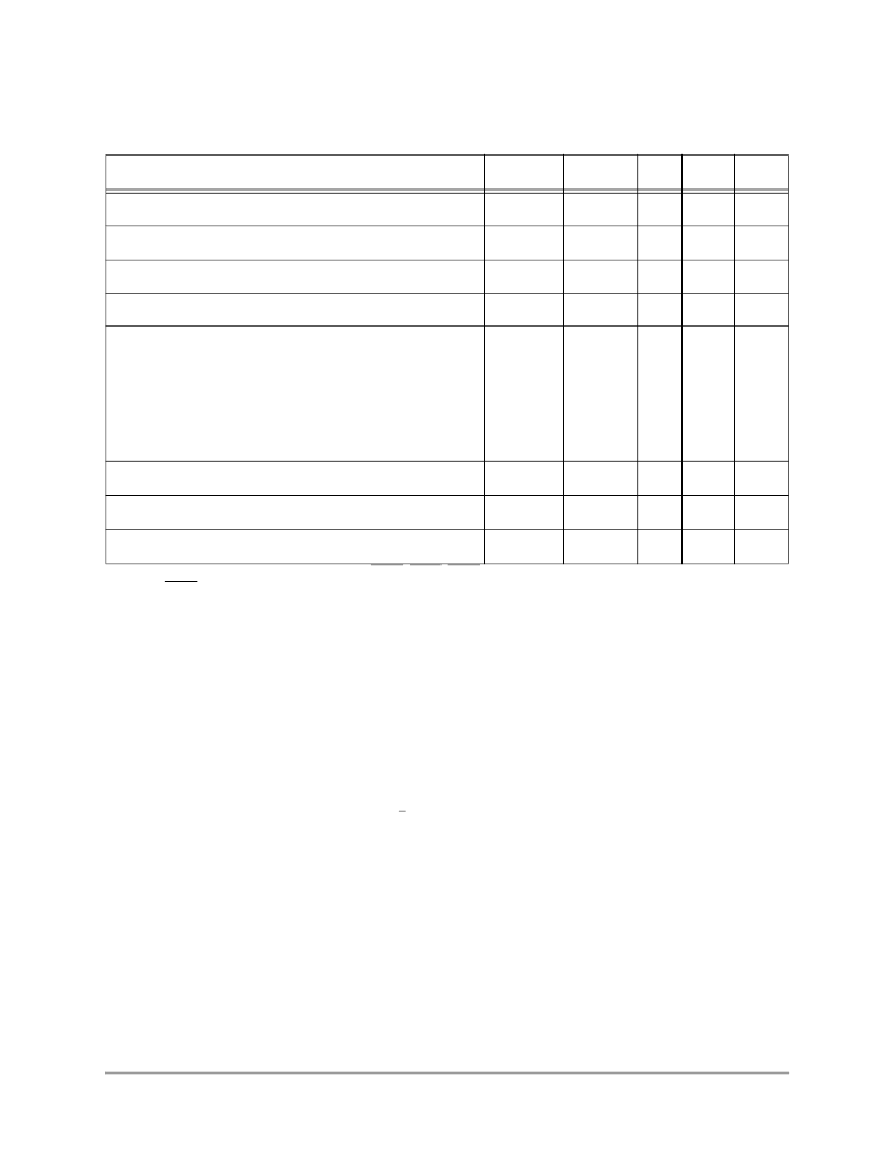
DC Electrical Characteristics
56F805 Technical Data
19
PWM pin output source current
3
I
OHP
10
—
—
mA
PWM pin output sink current
4
I
OLP
16
—
—
mA
Input capacitance
C
IN
—
8
—
pF
Output capacitance
C
OUT
—
12
—
pF
V
DD
supply current
I
DDT5
Run
6
—
126
152
mA
Wait
7
—
105
129
mA
Stop
—
60
84
mA
Low Voltage Interrupt, external power supply
8
V
EIO
2.4
2.7
3.0
V
Low Voltage Interrupt, internal power supply
9
V
EIC
2.0
2.2
2.4
V
Power on Reset
10
V
POR
—
1.7
2.0
V
1.
TCK, TRST, TMS, TDI, and MSCAN_RX
2.
Analog inputs are: ANA[0:7], XTAL and EXTAL. Specification assumes ADC is not sampling.
3.
PWM pin output source current measured with 50% duty cycle.
4.
PWM pin output sink current measured with 50% duty cycle.
5.
I
DDT
= I
DD
+ I
DDA
(Total supply current for V
DD
+ V
DDA
)
6.
Run (operating) I
DD
measured using 8MHz clock source. All inputs 0.2V from rail; outputs unloaded. All ports
configured as inputs; measured with all modules enabled.
7.
Wait I
DD
measured using external square wave clock source (f
osc
= 8MHz) into XTAL; all inputs 0.2V from rail; no
DC loads; less than 50pF on all outputs. C
L
= 20pF on EXTAL; all ports configured as inputs; EXTAL capacitance
linearly affects wait I
DD
; measured with PLL enabled.
8.
This low voltage interrupt monitors the V
DDA
external power supply. V
DDA
is generally connected to the same
potential as V
DD
via separate traces. If V
DDA
drops below V
EIO
, an interrupt is generated. Functionality of the device is
guaranteed under transient conditions when V
DDA
>V
EIO
(between the minimum specified V
DD
and the point when the
V
EIO
interrupt is generated).
9.
This low voltage interrupt monitors the internally regulated core power supply. If the output from the internal
voltage is regulator drops below V
EIC
, an interrupt is generated. Since the core logic supply is internally regulated, this
interrupt will not be generated unless the external power supply drops below the minimum specified value (3.0V).
10. Power
–
on reset occurs whenever the internally regulated 2.5V digital supply drops below 1.5V typical. While power
is ramping up, this signal remains active as long as the internal 2.5V is below 1.5V typical, no matter how long the ramp-
up rate is. The internally regulated voltage is typically 100mV less than V
DD
during ramp-up until 2.5V is reached, at
which time it self-regulates.
Schmitt Trigger inputs are: EXTBOOT, IRQA, IRQB, RESET, ISA0-2, FAULTA0-3, ISB0-2, FAULT0B-3, TCS,
Table 23. DC Electrical Characteristics (Continued)
Operating Conditions:
V
SS
= V
SSA
= 0 V, V
DD
= V
DDA
= 3.0–3.6 V, T
A
= –40
°
to +85
°
C, C
L
≤
50pF, f
op
= 80MHz
Characteristic
Symbol
Min
Typ
Max
Unit
F
Freescale Semiconductor, Inc.
For More Information On This Product,
Go to: www.freescale.com
n
.
相關(guān)PDF資料 |
PDF描述 |
|---|---|
| DSP56F807PY80E | 16-bit Digital Signal Controllers |
| DSP56F807VF80E | 16-bit Digital Signal Controllers |
| DSP56F807 | 16-bit Hybrid Controller(16位混合控制器) |
| DSP56F826BU80 | 16-bit Digital Signal Controllers |
| DSP56F826BU80E | 16-bit Digital Signal Controllers |
相關(guān)代理商/技術(shù)參數(shù) |
參數(shù)描述 |
|---|---|
| DSP56F805ACIM | 制造商:未知廠家 制造商全稱:未知廠家 功能描述:Targeting Document for the 56F805 3-Phase AC Induction Motor V/Hz Control |
| DSP56F805BLDCQE | 制造商:未知廠家 制造商全稱:未知廠家 功能描述:Targeting Document for the 56F805 BLDC Motor Control Application with Quadrature Encoder |
| DSP56F805D | 制造商:MOTOROLA 制造商全稱:Motorola, Inc 功能描述:16-bit Hybrid Controller |
| DSP56F805E | 制造商:FREESCALE 制造商全稱:Freescale Semiconductor, Inc 功能描述:16-bit Digital Signal Controllers |
| DSP56F805EVM | 功能描述:開發(fā)板和工具包 - 其他處理器 Evaluation Kit For DSP56F805 RoHS:否 制造商:Freescale Semiconductor 產(chǎn)品:Development Systems 工具用于評估:P3041 核心:e500mc 接口類型:I2C, SPI, USB 工作電源電壓: |
發(fā)布緊急采購,3分鐘左右您將得到回復(fù)。