- 您現(xiàn)在的位置:買(mǎi)賣(mài)IC網(wǎng) > PDF目錄378285 > ADCS9888 (National Semiconductor Corporation) 205/170/140 MSPS Video Analog Front End PDF資料下載
參數(shù)資料
| 型號(hào): | ADCS9888 |
| 廠商: | National Semiconductor Corporation |
| 英文描述: | 205/170/140 MSPS Video Analog Front End |
| 中文描述: | 205/170/140 MSPS的視頻模擬前端 |
| 文件頁(yè)數(shù): | 5/34頁(yè) |
| 文件大小: | 764K |
| 代理商: | ADCS9888 |
第1頁(yè)第2頁(yè)第3頁(yè)第4頁(yè)當(dāng)前第5頁(yè)第6頁(yè)第7頁(yè)第8頁(yè)第9頁(yè)第10頁(yè)第11頁(yè)第12頁(yè)第13頁(yè)第14頁(yè)第15頁(yè)第16頁(yè)第17頁(yè)第18頁(yè)第19頁(yè)第20頁(yè)第21頁(yè)第22頁(yè)第23頁(yè)第24頁(yè)第25頁(yè)第26頁(yè)第27頁(yè)第28頁(yè)第29頁(yè)第30頁(yè)第31頁(yè)第32頁(yè)第33頁(yè)第34頁(yè)
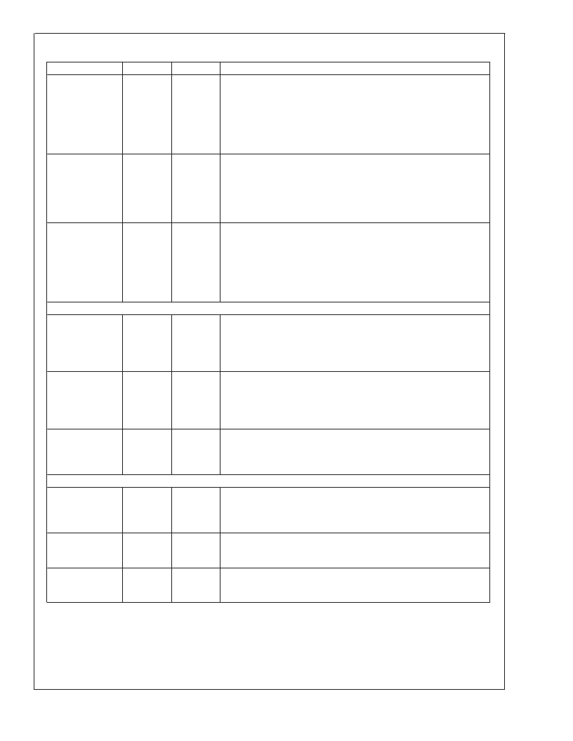
Pin Descriptions
(Continued)
Pin
Label
Type
Description
53
COAST
Digital Input PLL Clock Generator Coast Input. When enabled via Register 0Fh, Bit 5,
this input will cause the clock generator circuit to run open loop and ignore
the input reference clock. This is useful when operating with sync signals
that contain extra equalization pulses that must be ignored by the PLL. In
many cases, the internal VSOUT signal is used to provide the coast
control signal, but in some cases it is useful to provide an external COAST
control. Please refer to the applications section for more information.
Digital Input External Clock Input (Optional). This input can be used to provide an
external clock source instead of the internally generated clock. It is
enabled via Register 15h, Bit 0. When an external clock is used, most
other internal functions operate normally. When unused, this pin can be
connected to ground directly, or through a 10 k
resistor. The sampling
phase adjustment feature is operational when CKEXT is used.
Digital Input Sampling clock Inverting Input. This input can be used to invert the pixel
sampling clock, with respect to the normal phase of operation. This causes
the pixel sampling point to be shifted by 180 degrees in phase. Alternate
pixel sampling mode makes use of this feature by sampling at 1/2 the
incoming pixel rate, and switching the sampling phase by 180 degree
between alternate frames of video. When unused, this input should be
grounded. See the applications section for more information.
54
CKEXT
29
CKINV
Serial Interface
31
SDA
Digital I/O
Serial Control Interface Data Input/Output. The serial interface is used to
access the configuration and status registers in the ADCS9888. Mode and
Data information are transferred through the SDA pin from the host or
master device. Please refer to the applications section of the datasheet
under Serial Communications for more information.
Digital Input Serial Control Interface Clock Input. The clock input is controlled by the
host or master device, and is used to load in the data sent by the host,
and to clock data out of the ADCS9888. Please refer to the applications
section of the datasheet under Serial Communications for more
information.
Digital Input The least significant bit of the device serial address is selectable as 0 or 1
to allow up to 2 ADCS9888 devices to be connected on the same serial
interface. Please refer to the applications section of the datasheet under
Serial Communications for more information.
32
SCL
33
A0
Sync. Outputs
125
HSOUT
Digital
Output
Horizontal Sync Output. Internally generated and phase aligned horizontal
sync signal. This signal is used as a timing reference for the digital output
data stream. Please refer to the section on sync processing for more
information.
Vertical Sync Output. A delayed version of the input vertical
synchronization signal. Please refer to the section on sync processing for
more information.
Sync-On-Green Output. A logic level signal that is the output of the
Sync-On-Green slicer circuit. Please refer to the section on sync
processing for more information.
127
VSOUT
Digital
Output
126
SOGOUT
Digital
Output
A
www.national.com
5
相關(guān)PDF資料 |
PDF描述 |
|---|---|
| ADCV0831 | 8 Bit Serial I/O Low Voltage Low Power ADC with Auto Shutdown in a SOT Package(SOT封裝8位串行輸入/輸出低壓低功耗帶自動(dòng)關(guān)閉功能的A/D轉(zhuǎn)換器) |
| ADCV0831M6 | 8 Bit Serial I/O Low Voltage Low Power ADC with Auto Shutdown in a SOT Package |
| ADCV0831M6X | 8 Bit Serial I/O Low Voltage Low Power ADC with Auto Shutdown in a SOT Package |
| ADCV08832 | Low Voltage, 8-Bit Serial I/O CMOS A/D Converter with Sample/Hold Function |
| ADCV08832CIMX | Low Voltage, 8-Bit Serial I/O CMOS A/D Converter with Sample/Hold Function |
相關(guān)代理商/技術(shù)參數(shù) |
參數(shù)描述 |
|---|---|
| ADCS9888_05 | 制造商:NSC 制造商全稱:National Semiconductor 功能描述:205/170/140 MSPS Video Analog Front End |
| ADCS9888C WAF | 制造商:Texas Instruments 功能描述: |
| ADCS9888CVH-140 | 制造商:Texas Instruments 功能描述:140MSPS VIDEO AFE 9888 TQFP128 |
| ADCS9888CVH-140/NOPB | 功能描述:IC VIDEO AFE 140MSPS 128-PQFP RoHS:是 類別:集成電路 (IC) >> 數(shù)據(jù)采集 - 模擬前端 (AFE) 系列:- 產(chǎn)品培訓(xùn)模塊:Lead (SnPb) Finish for COTS Obsolescence Mitigation Program 標(biāo)準(zhǔn)包裝:2,500 系列:- 位數(shù):- 通道數(shù):2 功率(瓦特):- 電壓 - 電源,模擬:3 V ~ 3.6 V 電壓 - 電源,數(shù)字:3 V ~ 3.6 V 封裝/外殼:32-VFQFN 裸露焊盤(pán) 供應(yīng)商設(shè)備封裝:32-QFN(5x5) 包裝:帶卷 (TR) |
| ADCS9888CVH-170 | 制造商:Texas Instruments 功能描述:IC 170MSPS VIDEO AFE 9888 TQFP64 |
發(fā)布緊急采購(gòu),3分鐘左右您將得到回復(fù)。