- 您現(xiàn)在的位置:買賣IC網(wǎng) > PDF目錄373785 > ZL50015 (Zarlink Semiconductor Inc.) Enhanced 1 K Digital Switch with Stratum 4E DPLL PDF資料下載
參數(shù)資料
| 型號: | ZL50015 |
| 廠商: | Zarlink Semiconductor Inc. |
| 英文描述: | Enhanced 1 K Digital Switch with Stratum 4E DPLL |
| 中文描述: | 增強1K的數(shù)字交換與地層4E條數(shù)字鎖相環(huán) |
| 文件頁數(shù): | 24/122頁 |
| 文件大小: | 926K |
| 代理商: | ZL50015 |
第1頁第2頁第3頁第4頁第5頁第6頁第7頁第8頁第9頁第10頁第11頁第12頁第13頁第14頁第15頁第16頁第17頁第18頁第19頁第20頁第21頁第22頁第23頁當(dāng)前第24頁第25頁第26頁第27頁第28頁第29頁第30頁第31頁第32頁第33頁第34頁第35頁第36頁第37頁第38頁第39頁第40頁第41頁第42頁第43頁第44頁第45頁第46頁第47頁第48頁第49頁第50頁第51頁第52頁第53頁第54頁第55頁第56頁第57頁第58頁第59頁第60頁第61頁第62頁第63頁第64頁第65頁第66頁第67頁第68頁第69頁第70頁第71頁第72頁第73頁第74頁第75頁第76頁第77頁第78頁第79頁第80頁第81頁第82頁第83頁第84頁第85頁第86頁第87頁第88頁第89頁第90頁第91頁第92頁第93頁第94頁第95頁第96頁第97頁第98頁第99頁第100頁第101頁第102頁第103頁第104頁第105頁第106頁第107頁第108頁第109頁第110頁第111頁第112頁第113頁第114頁第115頁第116頁第117頁第118頁第119頁第120頁第121頁第122頁
ZL50015
Data Sheet
24
Zarlink Semiconductor Inc.
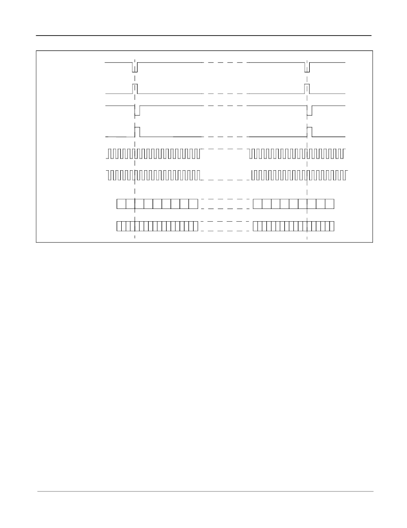
Figure 6 - Input Timing when CKIN1 - 0 = “00” in the CR
5.0 ST-BUS and GCI-Bus Timing
The ZL50015 is capable of operating using either the ST-BUS or GCI-Bus standards. The output timing that the
device generates is defined by the bus standard. In the ST-BUS standard, the output frame boundary is defined by
the falling edge of CKo while FPo is low. In the GCI-Bus standard, the frame boundary is defined by the rising edge
of CKo while FPo goes high. The data rates define the number of channels that are available in a 125
μ
s frame
pulse period.
By default, the ZL50015 is configured for ST-BUS input and output timing. To set the input timing to conform to the
GCI-Bus standard, FPINPOS (bit 9) and FPINP (bit 7) in the Control Register (CR) must be set. To set output timing
to conform to the GCI-Bus standard, FPO[n]P and FPO[n]POS must be set in the Output Clock and Frame Pulse
Selection Register (OCFSR). The CKO[n]P bits in the Output Clock and Frame Pulse Selection Register control the
polarity (positive-going or negative-going) of the output clocks.
6.0 Output Timing Generation
The ZL50015 generates frame pulse and clock timing. There are five output frame pulse pins (FPo0 - 3, 5) and six
output clock pins (CKo0 - 5). All output frame pulses are 8 kHz output signals. By default, the output frame
boundary is defined by the falling edge of the CKo0, while FPo0 is low. At the output frame boundary, the CKo1,
CKo2 and CKo3 output clocks will by default have a falling edge, while FPo1, FPo2 and FPo3 will be low. At the
output frame boundary, CKo4 will by default have a falling edge while FPo0 is low (CKo4 has no corresponding
output frame pulse). At the output frame boundary, CKo5 will by default have a rising edge while FPo5 (FPo_OFF2)
will be low. The duration of the frame pulse low cycle and the frequency of the corresponding output clock are
shown in Table 3 on page 25. Every frame pulse and clock output can be tristated by programming the enable bits
in the Internal Mode Selection (IMS) register.
FPi (61 ns)
FPINP = 0
FPINPOS = 0
FPi (61 ns)
FPINP = 1
FPINPOS = 0
FPi (61 ns)
FPINP = 0
FPINPOS = 1
FPi (61 ns)
FPINP = 1
FPINPOS = 1
CKi
(16.384 MHz)
CKINP = 0
CKi
(16.384 MHz)
CKINP = 1
STi
(8.192 Mbps)
Channel 0
Channel N = 127
6 5 4
3 2 1
3 2 1 0
5 4
7
6 5
7
1 0
STi
(16.384 Mbps)
Channel 0
Channel N = 255
6
7
4
5
2
3
0
1
6
7
4
5
2
3
2
3
0
1
6
7
4
5
2
3
6
7
4
5
2
3
0
1
2
3
0
1
S
G
相關(guān)PDF資料 |
PDF描述 |
|---|---|
| ZL50015GAC | Enhanced 1 K Digital Switch with Stratum 4E DPLL |
| ZL50015QCC | Enhanced 1 K Digital Switch with Stratum 4E DPLL |
| ZL50015QCC1 | Enhanced 1 K Digital Switch with Stratum 4E DPLL |
| ZL50018 | 2 K Digital Switch with Enhanced Stratum 3 DPLL |
| ZL50018GAC | 2 K Digital Switch with Enhanced Stratum 3 DPLL |
相關(guān)代理商/技術(shù)參數(shù) |
參數(shù)描述 |
|---|---|
| ZL50015_06 | 制造商:ZARLINK 制造商全稱:Zarlink Semiconductor Inc 功能描述:Enhanced 1 K Digital Switch with Stratum 4E DPLL |
| ZL50015GAC | 制造商:Microsemi Corporation 功能描述:Switch Fabric 1K x 1K 1.8V/3.3V 256-Pin BGA Tray 制造商:Microsemi Corporation 功能描述:SWIT FABRIC 1K X 1K 1.8V/3.3V 256BGA - Trays 制造商:Zarlink Semiconductor Inc 功能描述:SWIT FABRIC 1K X 1K 1.8V/3.3V 256BGA - Trays |
| ZL50015GAG2 | 制造商:Microsemi Corporation 功能描述:SWIT FABRIC 1K X 1K 1.8V/3.3V 256BGA - Trays 制造商:Zarlink Semiconductor Inc 功能描述:SWIT FABRIC 1K X 1K 1.8V/3.3V 256BGA - Trays |
| ZL50015QCC | 制造商:Microsemi Corporation 功能描述:SWIT FABRIC 1K X 1K 1.8V/3.3V 256LQFP - Trays |
| ZL50015QCC1 | 制造商:ZARLINK 制造商全稱:Zarlink Semiconductor Inc 功能描述:Enhanced 1 K Digital Switch with Stratum 4E DPLL |
發(fā)布緊急采購,3分鐘左右您將得到回復(fù)。