- 您現(xiàn)在的位置:買(mǎi)賣(mài)IC網(wǎng) > PDF目錄383961 > TMX320DM6443ZWT (Texas Instruments, Inc.) Digital Media System-on-Chip PDF資料下載
參數(shù)資料
| 型號(hào): | TMX320DM6443ZWT |
| 廠(chǎng)商: | Texas Instruments, Inc. |
| 英文描述: | Digital Media System-on-Chip |
| 中文描述: | 數(shù)字媒體系統(tǒng)片上 |
| 文件頁(yè)數(shù): | 119/221頁(yè) |
| 文件大小: | 1582K |
| 代理商: | TMX320DM6443ZWT |
第1頁(yè)第2頁(yè)第3頁(yè)第4頁(yè)第5頁(yè)第6頁(yè)第7頁(yè)第8頁(yè)第9頁(yè)第10頁(yè)第11頁(yè)第12頁(yè)第13頁(yè)第14頁(yè)第15頁(yè)第16頁(yè)第17頁(yè)第18頁(yè)第19頁(yè)第20頁(yè)第21頁(yè)第22頁(yè)第23頁(yè)第24頁(yè)第25頁(yè)第26頁(yè)第27頁(yè)第28頁(yè)第29頁(yè)第30頁(yè)第31頁(yè)第32頁(yè)第33頁(yè)第34頁(yè)第35頁(yè)第36頁(yè)第37頁(yè)第38頁(yè)第39頁(yè)第40頁(yè)第41頁(yè)第42頁(yè)第43頁(yè)第44頁(yè)第45頁(yè)第46頁(yè)第47頁(yè)第48頁(yè)第49頁(yè)第50頁(yè)第51頁(yè)第52頁(yè)第53頁(yè)第54頁(yè)第55頁(yè)第56頁(yè)第57頁(yè)第58頁(yè)第59頁(yè)第60頁(yè)第61頁(yè)第62頁(yè)第63頁(yè)第64頁(yè)第65頁(yè)第66頁(yè)第67頁(yè)第68頁(yè)第69頁(yè)第70頁(yè)第71頁(yè)第72頁(yè)第73頁(yè)第74頁(yè)第75頁(yè)第76頁(yè)第77頁(yè)第78頁(yè)第79頁(yè)第80頁(yè)第81頁(yè)第82頁(yè)第83頁(yè)第84頁(yè)第85頁(yè)第86頁(yè)第87頁(yè)第88頁(yè)第89頁(yè)第90頁(yè)第91頁(yè)第92頁(yè)第93頁(yè)第94頁(yè)第95頁(yè)第96頁(yè)第97頁(yè)第98頁(yè)第99頁(yè)第100頁(yè)第101頁(yè)第102頁(yè)第103頁(yè)第104頁(yè)第105頁(yè)第106頁(yè)第107頁(yè)第108頁(yè)第109頁(yè)第110頁(yè)第111頁(yè)第112頁(yè)第113頁(yè)第114頁(yè)第115頁(yè)第116頁(yè)第117頁(yè)第118頁(yè)當(dāng)前第119頁(yè)第120頁(yè)第121頁(yè)第122頁(yè)第123頁(yè)第124頁(yè)第125頁(yè)第126頁(yè)第127頁(yè)第128頁(yè)第129頁(yè)第130頁(yè)第131頁(yè)第132頁(yè)第133頁(yè)第134頁(yè)第135頁(yè)第136頁(yè)第137頁(yè)第138頁(yè)第139頁(yè)第140頁(yè)第141頁(yè)第142頁(yè)第143頁(yè)第144頁(yè)第145頁(yè)第146頁(yè)第147頁(yè)第148頁(yè)第149頁(yè)第150頁(yè)第151頁(yè)第152頁(yè)第153頁(yè)第154頁(yè)第155頁(yè)第156頁(yè)第157頁(yè)第158頁(yè)第159頁(yè)第160頁(yè)第161頁(yè)第162頁(yè)第163頁(yè)第164頁(yè)第165頁(yè)第166頁(yè)第167頁(yè)第168頁(yè)第169頁(yè)第170頁(yè)第171頁(yè)第172頁(yè)第173頁(yè)第174頁(yè)第175頁(yè)第176頁(yè)第177頁(yè)第178頁(yè)第179頁(yè)第180頁(yè)第181頁(yè)第182頁(yè)第183頁(yè)第184頁(yè)第185頁(yè)第186頁(yè)第187頁(yè)第188頁(yè)第189頁(yè)第190頁(yè)第191頁(yè)第192頁(yè)第193頁(yè)第194頁(yè)第195頁(yè)第196頁(yè)第197頁(yè)第198頁(yè)第199頁(yè)第200頁(yè)第201頁(yè)第202頁(yè)第203頁(yè)第204頁(yè)第205頁(yè)第206頁(yè)第207頁(yè)第208頁(yè)第209頁(yè)第210頁(yè)第211頁(yè)第212頁(yè)第213頁(yè)第214頁(yè)第215頁(yè)第216頁(yè)第217頁(yè)第218頁(yè)第219頁(yè)第220頁(yè)第221頁(yè)
www.ti.com
6.8.1
GPIO Peripheral Register Description(s)
TMS320DM6443
Digital Media System-on-Chip
SPRS282E–DECEMBER 2005–REVISED MARCH 2007
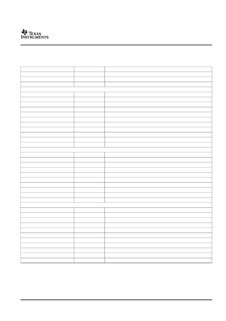
Table 6-25. GPIO Registers
HEX ADDRESS RANGE
0x01C6 7000
0x01C6 7004
0x01C6 7008
ACRONYM
PID
-
BINTEN
REGISTER NAME
Peripheral Identification Register
Reserved
GPIO interrupt per-bank enable
GPIO Banks 0 and 1
Reserved
GPIO Banks 0 and 1 Direction Register (GPIO[0:31])
GPIO Banks 0 and 1 Output Data Register (GPIO[0:31])
GPIO Banks 0 and 1 Set Data Register (GPIO[0:31])
GPIO Banks 0 and 1 Clear data for banks 0 and 1 (GPIO[0:31])
GPIO Banks 0 and 1 Input Data Register (GPIO[0:31])
SET_RIS_TRIG01
GPIO Banks 0 and 1 Set Rising Edge Interrupt Register (GPIO[0:31])
CLR_RIS_TRIG01
GPIO Banks 0 and 1 Clear Rising Edge Interrupt Register (GPIO[0:31])
SET_FAL_TRIG01
GPIO Banks 0 and 1 Set Falling Edge Interrupt Register (GPIO[0:31])
CLR_FAL_TRIG01
GPIO Banks 0 and 1 Clear Falling Edge Interrupt Register (GPIO[0:31])
INSTAT01
GPIO Banks 0 and 1 Interrupt Status Register (GPIO[0:31])
GPIO Banks 2 and 3
DIR23
GPIO Banks 2 and 3 Direction Register (GPIO[32:63])
OUT_DATA23
GPIO Banks 2 and 3 Output Data Register (GPIO[32:63])
SET_DATA23
GPIO Banks 2 and 3 Set Data Register (GPIO[32:63])
CLR_DATA23
GPIO Banks 2 and 3 Clear Data Register (GPIO[32:63])
IN_DATA23
GPIO Banks 2 and 3 Input Data Register (GPIO[32:63])
SET_RIS_TRIG23
GPIO Banks 2 and 3 Set Rising Edge Interrupt Register (GPIO[32:63])
CLR_RIS_TRIG23
GPIO Banks 2 and 3 Clear Rising Edge Interrupt Register (GPIO[32:63])
SET_FAL_TRIG23
GPIO Banks 2 and 3 Set Falling Edge Interrupt Register (GPIO[32:63])
CLR_FAL_TRIG23
GPIO Banks 2 and 3 Clear Falling Edge Interrupt Register (GPIO[32:63])
INSTAT23
GPIO Banks 2 and 3 Interrupt Status Register (GPIO[32:63])
GPIO Bank 4
DIR4
GPIO Bank 4 Direction Register (GPIO[64:70])
OUT_DATA4
GPIO Bank 4 Output Data Register (GPIO[64:70])
SET_DATA4
GPIO Bank 4 Set Data Register (GPIO[64:70])
CLR_DATA4
GPIO Bank 4 Clear Data Register (GPIO[64:70])
IN_DATA4
GPIO Bank 4 Input Data Register (GPIO[64:70])
SET_RIS_TRIG4
GPIO Bank 4 Set Rising Edge Interrupt Register (GPIO[64:70])
CLR_RIS_TRIG4
GPIO Bank 4 Clear Rising Edge Interrupt Register (GPIO[64:70])
SET_FAL_TRIG4
GPIO Bank 4 Set Falling Edge Interrupt Register (GPIO[64:70])
CLR_FAL_TRIG4
GPIO Bank 4 Clear Falling Edge Interrupt Register (GPIO[64:70])
INSTAT4
GPIO Bank 4 Interrupt Status Register (GPIO[64:70])
-
Reserved
0x01C6 700C
0x01C6 7010
0x01C6 7014
0x01C6 7018
0x01C6 701C
0x01C6 7020
0x01C6 7024
0x01C6 7028
0x01C6 702C
0x01C6 7030
0x01C6 7034
-
DIR01
OUT_DATA01
SET_DATA01
CLR_DATA01
IN_DATA01
0x01C6 7038
0x01C6 703C
0x01C6 7040
0x01C6 7044
0x01C6 7048
0x01C6 704C
0x01C6 7050
0x01C6 7054
0x01C6 7058
0x01C6 705C
0x01C6 7060
0x01C6 7064
0x01C6 7068
0x01C6 706C
0x01C6 7070
0x01C6 7074
0x01C6 7078
0x01C6 707C
0x01C6 7080
0x01C6 7084
0x01C6 7088 - 0x01C6 7FFF
Submit Documentation Feedback
Peripheral and Electrical Specifications
119
相關(guān)PDF資料 |
PDF描述 |
|---|---|
| TMS320DM647_08 | Digital Media Processor |
| TMS320DM647ZUT720 | Digital Media Processor |
| TMS320DM647ZUT900 | Digital Media Processor |
| TMS320DM648ZUT720 | Digital Media Processor |
| TMS320DM648ZUT900 | Digital Media Processor |
相關(guān)代理商/技術(shù)參數(shù) |
參數(shù)描述 |
|---|---|
| TMX320DM6444AZWT | 制造商:Texas Instruments 功能描述:TMS320DM6443, TMS320DM6444 DIGITAL MEDIA SOC DATA SHEET - Trays |
| TMX320DM6446AZWT | 制造商:Texas Instruments 功能描述: |
| TMX320DM6446AZWT8 | 制造商:Texas Instruments 功能描述:DAVINCI REL 2.1 810 MHZ - Trays |
| TMX320DM6446AZWTA | 制造商:Texas Instruments 功能描述:DAVINCI DIGITAL MEDIA SYSTEM-ON-CHIP - Trays |
| TMX320DM6446BZWT | 制造商:Texas Instruments 功能描述:SYS-ON-CHIP PROCESSOR 361PIN NFBGA - Trays |
發(fā)布緊急采購(gòu),3分鐘左右您將得到回復(fù)。