- 您現(xiàn)在的位置:買賣IC網(wǎng) > PDF目錄383961 > TMX320DM6443ZWT (Texas Instruments, Inc.) Digital Media System-on-Chip PDF資料下載
參數(shù)資料
| 型號(hào): | TMX320DM6443ZWT |
| 廠商: | Texas Instruments, Inc. |
| 英文描述: | Digital Media System-on-Chip |
| 中文描述: | 數(shù)字媒體系統(tǒng)片上 |
| 文件頁數(shù): | 106/221頁 |
| 文件大小: | 1582K |
| 代理商: | TMX320DM6443ZWT |
第1頁第2頁第3頁第4頁第5頁第6頁第7頁第8頁第9頁第10頁第11頁第12頁第13頁第14頁第15頁第16頁第17頁第18頁第19頁第20頁第21頁第22頁第23頁第24頁第25頁第26頁第27頁第28頁第29頁第30頁第31頁第32頁第33頁第34頁第35頁第36頁第37頁第38頁第39頁第40頁第41頁第42頁第43頁第44頁第45頁第46頁第47頁第48頁第49頁第50頁第51頁第52頁第53頁第54頁第55頁第56頁第57頁第58頁第59頁第60頁第61頁第62頁第63頁第64頁第65頁第66頁第67頁第68頁第69頁第70頁第71頁第72頁第73頁第74頁第75頁第76頁第77頁第78頁第79頁第80頁第81頁第82頁第83頁第84頁第85頁第86頁第87頁第88頁第89頁第90頁第91頁第92頁第93頁第94頁第95頁第96頁第97頁第98頁第99頁第100頁第101頁第102頁第103頁第104頁第105頁當(dāng)前第106頁第107頁第108頁第109頁第110頁第111頁第112頁第113頁第114頁第115頁第116頁第117頁第118頁第119頁第120頁第121頁第122頁第123頁第124頁第125頁第126頁第127頁第128頁第129頁第130頁第131頁第132頁第133頁第134頁第135頁第136頁第137頁第138頁第139頁第140頁第141頁第142頁第143頁第144頁第145頁第146頁第147頁第148頁第149頁第150頁第151頁第152頁第153頁第154頁第155頁第156頁第157頁第158頁第159頁第160頁第161頁第162頁第163頁第164頁第165頁第166頁第167頁第168頁第169頁第170頁第171頁第172頁第173頁第174頁第175頁第176頁第177頁第178頁第179頁第180頁第181頁第182頁第183頁第184頁第185頁第186頁第187頁第188頁第189頁第190頁第191頁第192頁第193頁第194頁第195頁第196頁第197頁第198頁第199頁第200頁第201頁第202頁第203頁第204頁第205頁第206頁第207頁第208頁第209頁第210頁第211頁第212頁第213頁第214頁第215頁第216頁第217頁第218頁第219頁第220頁第221頁
www.ti.com
6.6.2
Clock PLL Considerations with External Clock Sources
TMS320DM6443
Digital Media System-on-Chip
SPRS282E–DECEMBER 2005–REVISED MARCH 2007
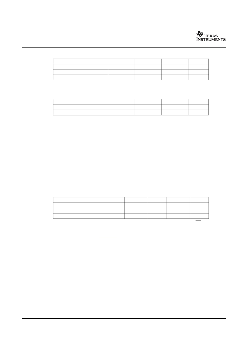
Table 6-13. PLLC1 Clock Frequency Ranges
CLOCK SIGNAL NAME
MIN
20
400
MAX
30
600
600
UNIT
MHz
MHz
MHz
MXI/CLKIN
(1)
PLLOUT
SYSCLK1 (CLKDIV1 Domain)
At 1.2-V CV
DD
(1)
MXI/CLKIN input clock is used for both PLL Controllers (PLLC1 and PLLC2).
Table 6-14. PLLC2 Clock Frequency Ranges
CLOCK SIGNAL NAME
MIN
20
400
MAX
30
900
UNIT
MHz
MHz
MXI/CLKIN
(1)
PLLOUT
At 1.2-V CV
DD
(1)
MXI/CLKIN input clock is used for both PLL Controllers (PLLC1 and PLLC2).
Both PLL1 and PLL2 have stabilization, lock, and reset timing requirements that
must
be followed.
The PLL stabilization time is the amount of time that
must
be allotted for the internal PLL regulators to
become stable after the PLL is powered up (after PLLCTL.PLLPWRDN bit goes through a 1-to-0
transition). The PLL should
not
be operated until this stabilization time has expired. This stabilization step
must
be applied after these resets—a Power-on Reset, a Warm Reset, or a Max Reset, as the
PLLCTL.PLLPWRDN bit resets to a "1". For the PLL stabliziation time value, see
Table 6-15
.
The PLL reset time is the amount of wait time needed for the PLL to properly reset (writing PLLRST = 0)
before bringing the PLL out of reset (writing PLLRST = 1). For the PLL reset time value, see
Table 6-15
.
The PLL lock time is the amount of time needed from when the PLL is taken out of reset (PLLRST = 1
with PLLEN = 0) to when to when the PLL controller can be switched to PLL mode (PLLEN = 1). For the
PLL lock time value, see
Table 6-15
.
Table 6-15. PLL1 and PLL2 Stabilization, Lock, and Reset Times
PLL STABILIZATION/LOCK/RESET TIME
PLL Stabilization Time
PLL Lock Time
PLL Reset Time
MIN
150
TYP
MAX
UNIT
μ
s
ns
ns
2000C
(1)
128C
(1)
(1)
C = CLKIN cycle time in ns. For example, when MXI/CLKIN frequency is 27 MHz, use C = 37.037 ns.
For details on the PLL initialization software sequence, see the
TMS320DM6443 DMSoC ARM Subsystem
Reference Guide
(literature number
SPRUE14
).
If the internal oscillator is bypassed, to minimize the clock jitter a single clean power supply should power
both the DM6443 device and the external clock oscillator circuit. The minimum CLKIN rise and fall times
should also be observed. For the input clock timing requirements, see
Section 6.6.3
,
Clock PLL Electrical
Data/Timing (Input and Output Clocks)
.
Rise/fall times, duty cycles (high/low pulse durations), and the load capacitance of the external clock
source must meet the device requirements in this data manual (see
Section 5.3
,
Electrical Characteristics
Over Recommended Ranges of Supply Voltage and Operating Case Temperature
and
Section 6.6.3
,
Clock PLL Electrical Data/Timing (Input and Output Clocks)
.
Peripheral and Electrical Specifications
106
Submit Documentation Feedback
相關(guān)PDF資料 |
PDF描述 |
|---|---|
| TMS320DM647_08 | Digital Media Processor |
| TMS320DM647ZUT720 | Digital Media Processor |
| TMS320DM647ZUT900 | Digital Media Processor |
| TMS320DM648ZUT720 | Digital Media Processor |
| TMS320DM648ZUT900 | Digital Media Processor |
相關(guān)代理商/技術(shù)參數(shù) |
參數(shù)描述 |
|---|---|
| TMX320DM6444AZWT | 制造商:Texas Instruments 功能描述:TMS320DM6443, TMS320DM6444 DIGITAL MEDIA SOC DATA SHEET - Trays |
| TMX320DM6446AZWT | 制造商:Texas Instruments 功能描述: |
| TMX320DM6446AZWT8 | 制造商:Texas Instruments 功能描述:DAVINCI REL 2.1 810 MHZ - Trays |
| TMX320DM6446AZWTA | 制造商:Texas Instruments 功能描述:DAVINCI DIGITAL MEDIA SYSTEM-ON-CHIP - Trays |
| TMX320DM6446BZWT | 制造商:Texas Instruments 功能描述:SYS-ON-CHIP PROCESSOR 361PIN NFBGA - Trays |
發(fā)布緊急采購,3分鐘左右您將得到回復(fù)。