- 您現(xiàn)在的位置:買賣IC網(wǎng) > PDF目錄372122 > SC28L202 (NXP Semiconductors N.V.) Dual universal asynchronous receiver/transmitter DUART PDF資料下載
參數(shù)資料
| 型號(hào): | SC28L202 |
| 廠商: | NXP Semiconductors N.V. |
| 英文描述: | Dual universal asynchronous receiver/transmitter DUART |
| 中文描述: | 雙路通用異步接收器/發(fā)送器杜阿爾特 |
| 文件頁數(shù): | 10/77頁 |
| 文件大?。?/td> | 531K |
| 代理商: | SC28L202 |
第1頁第2頁第3頁第4頁第5頁第6頁第7頁第8頁第9頁當(dāng)前第10頁第11頁第12頁第13頁第14頁第15頁第16頁第17頁第18頁第19頁第20頁第21頁第22頁第23頁第24頁第25頁第26頁第27頁第28頁第29頁第30頁第31頁第32頁第33頁第34頁第35頁第36頁第37頁第38頁第39頁第40頁第41頁第42頁第43頁第44頁第45頁第46頁第47頁第48頁第49頁第50頁第51頁第52頁第53頁第54頁第55頁第56頁第57頁第58頁第59頁第60頁第61頁第62頁第63頁第64頁第65頁第66頁第67頁第68頁第69頁第70頁第71頁第72頁第73頁第74頁第75頁第76頁第77頁
Philips Semiconductors
Objective specification
SC28L202
Dual UART
2000 Feb 10
4
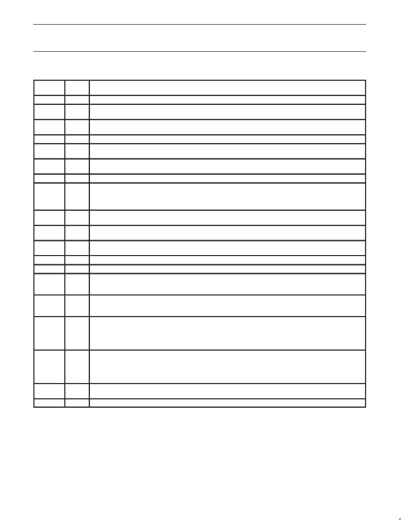
CONFIGURATION FOR 68XXX BUS INTERFACE (MOTOROLA)
Symbol
Pin
type
Name and Function
I/M
I
Bus Configuration: When low configures the bus interface to the Conditions shown in this table.
D0–D7
I/O
Data Bus: Bi–directional 3–State data bus used to transfer commands, data and status between the DUART and the
CPU. D0 is the least significant bit.
CSN
I
Chip Enable: Active–Low input signal. When Low, data transfers between the CPU and the DUART are enabled on
D0–D7 as controlled by the R/WN and A0–A6 inputs. When High, places the D0–D7 lines in the 3–State condition.
R/WN
I
Read/Write: Input Signal. When CSN is low R/WN high input a read cycle, when low a write cycle.
IACKN
I
Interrupt Acknowledge: Active low input indicates an interrupt acknowledge cycle. Usually asserted by the CPU in
response to an interrupt request. When asserted places the interrupt vector on the bus and asserts DACKN.
DACKN
O
Data Transfer Acknowledge: A 3–State active –low output asserted in a write, read, or interrupt acknowledge cycle to
indicate proper transfer of data between the CPU and the DUART.
A6–A0
I
Address Inputs: Select the DUART internal registers and ports for read/write operations.
RESETN
I
Reset: A low level clears internal registers (SR A , SR B, IMR, ISR, OPR, OPCR), places I/O[7:0] A and B at high
impedance input state, stops the counter/timer, and puts Channels A and B in the inactive state, with the TxD A and
TxD B outputs in the mark (High) state. Sets MR pointer to MR1, 9600 baud, 1 start, no parity and 1 stop bit(s). (See
Reset Table)
IRQN
O
Interrupt Request: Active–Low, open–drain, output which signals the CPU that one or more of the eighteen (18)
maskable interrupting conditions are true.
X1 / Sclk
I
Crystal 1: Crystal or external clock input. A crystal or clock of the specified limits must be supplied at all times. When
a crystal is used, a capacitor must be connected from this pin to ground (see Figure 9).
X2
O
Crystal 2: Connection for other side of the crystal. When a crystal is used, a capacitor must be connected from this
pin to ground (see Figure 9)
.
If Sclk is driven from an external source, this pin must be left open.
RxD A
I
Channel A Receiver Serial Data Input: The least significant bit is received first. “Mark” is High; “space” is Low.
RxD B
I
Channel B Receiver Serial Data Input: The least significant bit is received first. “Mark” is High; “space” is Low.
TxD A
O
Channel A Transmitter Serial Data Output: The least significant bit is transmitted first. This output is held in the
“mark” condition when the transmitter is disabled, idle or when operating in local loop back mode. “Mark” is High;
“space” is Low.
TxD B
O
Channel B Transmitter Serial Data Output: The least significant bit is transmitted first. This output is held in the ‘mark’
condition when the transmitter is disabled, idle, or when operating in local loop back mode. ‘Mark’ is High; ‘space’ is
Low.
I/O[7:0]A
I/O
General–purpose input and output ports channel A: The character of these pins is controlled by I/OPCR. They may
be inputs or outputs and will present many internal clocks and interrupt signals: RTS, CTS, DTR, DSR etc. All have
change of state detectors and the input is always active. These pins are set to input only when addressed from the
low order 16 address space. When these pins are configured for interrupt type signals (RxRDY, TxRDY, C/TRDY)
They switch to open drain outputs.
I/O[7:0}B
I/O
General–purpose input and output ports channel B: The character of these pins is controlled by I/OPCR. They may
be inputs or outputs and will present many internal clocks and interrupt signals: RTS, CTS, DTR, DSR etc. All have
change of state detectors and the input is always active. These pins are set to output only when addressed from the
low order 16 address space. When these pins are configured for interrupt type signals (RxRDY, TxRDY, C/TRDY)
They switch to open drain outputs
Vcc
Power
Power Supply: +3.3 or +5V supply input
±
10% (4 Vcc Pins) ). Operation is assured from 2.97 to 5.5 volts. Timing
parameters are specified with respect to the Vcc being at 3.3 of 5.0 volts +/– 10%
Vss
Power
Ground (5 Vss Pins)
相關(guān)PDF資料 |
PDF描述 |
|---|---|
| SC28L202A1B | Dual universal asynchronous receiver/transmitter DUART |
| SC28L202A1D | Dual universal asynchronous receiver/transmitter DUART |
| SC431CS8DE2 | Analog IC |
| SC431CS8DE3 | Analog IC |
| SC431CS8DF1 | Analog IC |
相關(guān)代理商/技術(shù)參數(shù) |
參數(shù)描述 |
|---|---|
| SC28L202A1 | 制造商:PHILIPS 制造商全稱:NXP Semiconductors 功能描述:Dual universal asynchronous receiver/transmitter DUART |
| SC28L202A1B | 制造商:PHILIPS 制造商全稱:NXP Semiconductors 功能描述:Dual universal asynchronous receiver/transmitter DUART |
| SC28L202A1D | 制造商:PHILIPS 制造商全稱:NXP Semiconductors 功能描述:Dual universal asynchronous receiver/transmitter DUART |
| SC28L202A1DGG | 功能描述:UART 接口集成電路 3-5V 2CH UART 3MBPS 256B FIFO RoHS:否 制造商:Texas Instruments 通道數(shù)量:2 數(shù)據(jù)速率:3 Mbps 電源電壓-最大:3.6 V 電源電壓-最小:2.7 V 電源電流:20 mA 最大工作溫度:+ 85 C 最小工作溫度:- 40 C 封裝 / 箱體:LQFP-48 封裝:Reel |
| SC28L202A1DGG,112 | 功能描述:UART 接口集成電路 3-5V 2CH UART 3MBPS RoHS:否 制造商:Texas Instruments 通道數(shù)量:2 數(shù)據(jù)速率:3 Mbps 電源電壓-最大:3.6 V 電源電壓-最小:2.7 V 電源電流:20 mA 最大工作溫度:+ 85 C 最小工作溫度:- 40 C 封裝 / 箱體:LQFP-48 封裝:Reel |
發(fā)布緊急采購,3分鐘左右您將得到回復(fù)。