- 您現在的位置:買賣IC網 > PDF目錄378055 > PM7341 (PMC-SIERRA INC) S/UNI INVERSE MULTIPLEXING FOR ATM, 84 LINKS PDF資料下載
參數資料
| 型號: | PM7341 |
| 廠商: | PMC-SIERRA INC |
| 元件分類: | 數字傳輸電路 |
| 英文描述: | S/UNI INVERSE MULTIPLEXING FOR ATM, 84 LINKS |
| 中文描述: | ATM/SONET/SDH SUPPORT CIRCUIT, PBGA416 |
| 封裝: | 27 X 27 MM, 2.28 MM HEIGHT, PLASTIC, BGA-416 |
| 文件頁數: | 390/413頁 |
| 文件大小: | 3291K |
| 代理商: | PM7341 |
第1頁第2頁第3頁第4頁第5頁第6頁第7頁第8頁第9頁第10頁第11頁第12頁第13頁第14頁第15頁第16頁第17頁第18頁第19頁第20頁第21頁第22頁第23頁第24頁第25頁第26頁第27頁第28頁第29頁第30頁第31頁第32頁第33頁第34頁第35頁第36頁第37頁第38頁第39頁第40頁第41頁第42頁第43頁第44頁第45頁第46頁第47頁第48頁第49頁第50頁第51頁第52頁第53頁第54頁第55頁第56頁第57頁第58頁第59頁第60頁第61頁第62頁第63頁第64頁第65頁第66頁第67頁第68頁第69頁第70頁第71頁第72頁第73頁第74頁第75頁第76頁第77頁第78頁第79頁第80頁第81頁第82頁第83頁第84頁第85頁第86頁第87頁第88頁第89頁第90頁第91頁第92頁第93頁第94頁第95頁第96頁第97頁第98頁第99頁第100頁第101頁第102頁第103頁第104頁第105頁第106頁第107頁第108頁第109頁第110頁第111頁第112頁第113頁第114頁第115頁第116頁第117頁第118頁第119頁第120頁第121頁第122頁第123頁第124頁第125頁第126頁第127頁第128頁第129頁第130頁第131頁第132頁第133頁第134頁第135頁第136頁第137頁第138頁第139頁第140頁第141頁第142頁第143頁第144頁第145頁第146頁第147頁第148頁第149頁第150頁第151頁第152頁第153頁第154頁第155頁第156頁第157頁第158頁第159頁第160頁第161頁第162頁第163頁第164頁第165頁第166頁第167頁第168頁第169頁第170頁第171頁第172頁第173頁第174頁第175頁第176頁第177頁第178頁第179頁第180頁第181頁第182頁第183頁第184頁第185頁第186頁第187頁第188頁第189頁第190頁第191頁第192頁第193頁第194頁第195頁第196頁第197頁第198頁第199頁第200頁第201頁第202頁第203頁第204頁第205頁第206頁第207頁第208頁第209頁第210頁第211頁第212頁第213頁第214頁第215頁第216頁第217頁第218頁第219頁第220頁第221頁第222頁第223頁第224頁第225頁第226頁第227頁第228頁第229頁第230頁第231頁第232頁第233頁第234頁第235頁第236頁第237頁第238頁第239頁第240頁第241頁第242頁第243頁第244頁第245頁第246頁第247頁第248頁第249頁第250頁第251頁第252頁第253頁第254頁第255頁第256頁第257頁第258頁第259頁第260頁第261頁第262頁第263頁第264頁第265頁第266頁第267頁第268頁第269頁第270頁第271頁第272頁第273頁第274頁第275頁第276頁第277頁第278頁第279頁第280頁第281頁第282頁第283頁第284頁第285頁第286頁第287頁第288頁第289頁第290頁第291頁第292頁第293頁第294頁第295頁第296頁第297頁第298頁第299頁第300頁第301頁第302頁第303頁第304頁第305頁第306頁第307頁第308頁第309頁第310頁第311頁第312頁第313頁第314頁第315頁第316頁第317頁第318頁第319頁第320頁第321頁第322頁第323頁第324頁第325頁第326頁第327頁第328頁第329頁第330頁第331頁第332頁第333頁第334頁第335頁第336頁第337頁第338頁第339頁第340頁第341頁第342頁第343頁第344頁第345頁第346頁第347頁第348頁第349頁第350頁第351頁第352頁第353頁第354頁第355頁第356頁第357頁第358頁第359頁第360頁第361頁第362頁第363頁第364頁第365頁第366頁第367頁第368頁第369頁第370頁第371頁第372頁第373頁第374頁第375頁第376頁第377頁第378頁第379頁第380頁第381頁第382頁第383頁第384頁第385頁第386頁第387頁第388頁第389頁當前第390頁第391頁第392頁第393頁第394頁第395頁第396頁第397頁第398頁第399頁第400頁第401頁第402頁第403頁第404頁第405頁第406頁第407頁第408頁第409頁第410頁第411頁第412頁第413頁
PRELIMINARY
INVERSE MULTIPLEXING OVER ATM
PM7341 S/UNI-IMA-84
DATASHEET
PMC-2000223
ISSUE 4
INVERSE MULTIPLEXING OVER ATM
PROPRIETARY AND CONFIDENTIAL TO PMC-SIERRA, INC., AND FOR ITS CUSTOMERS’ INTERNAL USE
392
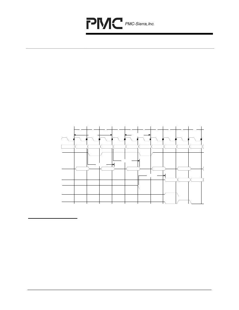
13.5.5 Any-PHY Receive Slave Interface
Figure 41 gives an example of the functional timing of the receive interface when
configured as an Any-PHY compliant receive slave. The interface responds to the
polling of address “IMA” (which matches the address defined by the Receive
Any-PHY/UTOPIA Config register) by asserting RPA when it is capable of
delivering a complete cell. The Any-PHY master repolls addresses until it
receives an asserted RPA. As a result, the master re-selects the same RADR
again during the last cycle RENB is high to initiate a transfer. Once transfer is
initiated, RENB must remain asserted until the last data is received.
Figure 41
- Any-PHY Receive Slave
1
2
3
4
5
6
7
8
9
10
1F
IMA-AD
1F
PHY-Y
1F
IMA-AD
1F
PHY-Z
1F
PHY-Z
PHY-A
PHY-Z
IMA-ADR
PHY-Y
IMA-ADR
PHY-Z
IMA Add
Data 0
Data 1
2 RCLK
2 RCLK
2 RCLK
Selection
Polling
RCLK
RADR[4:0]
RCSB
RPA
RDAT[m:0], RPRTY
RENB
RSX
RSOP
13.6 SDRAM Interface
The following three diagrams depict the timing for signals destined for the pins of
the SDRAM during the Activate-Read (with Auto-precharge), Activate-Write (with
Auto-precharge), and Auto-refresh command sequences and Power-Up and
Initialization Sequence.. The cbcmd signal is not an actual signal; it merely
represents the memory access command formed by the combination of the
individual SDRAM control signals (e.g., cbcsb and cbrasb). Also note that
reads/writes of cell buffers are always done in bursts of eight words, with 4 bursts
per cells; the first and third bursts involve the even banks and the second and
fourth bursts involve the odd banks in the SDRAM.
相關PDF資料 |
PDF描述 |
|---|---|
| PM7342 | 32 Link Inverse Multiplexer for ATM (IMA) / UNI PHY |
| PM7344 | SATURN QUAD T1/E1 MULTI-PHY USER NETWORK INTERFACE DEVICE |
| PM7345 | SATURN User Network Interface for PDH Applications |
| PM7346 | SATURN QUAD USER NETWORK INTERFACE FOR J2, E3, T3 |
| PM7347 | SATURN USER NETWORK INTERFACE for J2/E3/T3 |
相關代理商/技術參數 |
參數描述 |
|---|---|
| PM7342 | 制造商:PMC 制造商全稱:PMC 功能描述:32 Link Inverse Multiplexer for ATM (IMA) / UNI PHY |
| PM7344 | 制造商:PMC 制造商全稱:PMC 功能描述:SATURN QUAD T1/E1 MULTI-PHY USER NETWORK INTERFACE DEVICE |
發(fā)布緊急采購,3分鐘左右您將得到回復。