- 您現(xiàn)在的位置:買(mǎi)賣(mài)IC網(wǎng) > PDF目錄11733 > ORT82G5-2FN680I (Lattice Semiconductor Corporation)IC TRANCEIVERS FPSC 680FPBGA PDF資料下載
參數(shù)資料
| 型號(hào): | ORT82G5-2FN680I |
| 廠商: | Lattice Semiconductor Corporation |
| 文件頁(yè)數(shù): | 106/119頁(yè) |
| 文件大小: | 0K |
| 描述: | IC TRANCEIVERS FPSC 680FPBGA |
| 產(chǎn)品變化通告: | Product Discontinuation 01/Aug/2011 |
| 標(biāo)準(zhǔn)包裝: | 24 |
| 系列: | * |
第1頁(yè)第2頁(yè)第3頁(yè)第4頁(yè)第5頁(yè)第6頁(yè)第7頁(yè)第8頁(yè)第9頁(yè)第10頁(yè)第11頁(yè)第12頁(yè)第13頁(yè)第14頁(yè)第15頁(yè)第16頁(yè)第17頁(yè)第18頁(yè)第19頁(yè)第20頁(yè)第21頁(yè)第22頁(yè)第23頁(yè)第24頁(yè)第25頁(yè)第26頁(yè)第27頁(yè)第28頁(yè)第29頁(yè)第30頁(yè)第31頁(yè)第32頁(yè)第33頁(yè)第34頁(yè)第35頁(yè)第36頁(yè)第37頁(yè)第38頁(yè)第39頁(yè)第40頁(yè)第41頁(yè)第42頁(yè)第43頁(yè)第44頁(yè)第45頁(yè)第46頁(yè)第47頁(yè)第48頁(yè)第49頁(yè)第50頁(yè)第51頁(yè)第52頁(yè)第53頁(yè)第54頁(yè)第55頁(yè)第56頁(yè)第57頁(yè)第58頁(yè)第59頁(yè)第60頁(yè)第61頁(yè)第62頁(yè)第63頁(yè)第64頁(yè)第65頁(yè)第66頁(yè)第67頁(yè)第68頁(yè)第69頁(yè)第70頁(yè)第71頁(yè)第72頁(yè)第73頁(yè)第74頁(yè)第75頁(yè)第76頁(yè)第77頁(yè)第78頁(yè)第79頁(yè)第80頁(yè)第81頁(yè)第82頁(yè)第83頁(yè)第84頁(yè)第85頁(yè)第86頁(yè)第87頁(yè)第88頁(yè)第89頁(yè)第90頁(yè)第91頁(yè)第92頁(yè)第93頁(yè)第94頁(yè)第95頁(yè)第96頁(yè)第97頁(yè)第98頁(yè)第99頁(yè)第100頁(yè)第101頁(yè)第102頁(yè)第103頁(yè)第104頁(yè)第105頁(yè)當(dāng)前第106頁(yè)第107頁(yè)第108頁(yè)第109頁(yè)第110頁(yè)第111頁(yè)第112頁(yè)第113頁(yè)第114頁(yè)第115頁(yè)第116頁(yè)第117頁(yè)第118頁(yè)第119頁(yè)
Lattice Semiconductor
ORCA ORT42G5 and ORT82G5 Data Sheet
87
Package Information
Package Pinouts
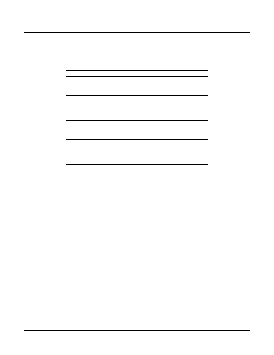
Table 43 provides the number of user-programmable I/Os available for each package.
Table 43. I/O Summary
Table 44 and Table 45 provide the package pin and pin function for the ORT42G5 and ORT82G5 FPSC and pack-
ages. The bond pad name is identied in the PIO nomenclature used in the ispLEVER System software design edi-
tor. The Bank column provides information as to which output voltage level bank the given pin is in. The Group
column provides information as to the group of pins the given pin is in. This is used to show which VREF pin is used
to provide the reference voltage for single-ended limited-swing I/Os. If none of these buffer types (such as SSTL,
GTL, HSTL) are used in a given group, then the VREF pin is available as an I/O pin.
When the number of FPGA bond pads exceeds the number of package pins, bond pads are unused. When the
number of package pins exceeds the number of bond pads, package pins are left unconnected (no connects).
When a package pin is to be left as a no connect for a specic die, it is indicated as a note in the device column for
the FPGA. The tables provide no information on unused pads.
As shown in the pair columns in Table 38, differential pairs and physical locations are numbered within each bank
(e.g., L19C-A0 is the nineteenth pair in an associated bank). A ‘C’ indicates complementary differential, whereas a
‘T’ indicates true differential. An _A0 indicates the physical location of adjacent balls in either the horizontal or ver-
tical direction. Other physical indicators are as follows:
_A1 indicates one ball between pairs.
_A2 indicates two balls between pairs.
_D0 indicates balls are diagonally adjacent.
_D1 indicates balls are diagonally adjacent, separated by one physical ball.
VREF pins, shown in the Pin Description columns in Table 44 and Table 45, are associated to the bank and group
(e.g., VREF_TL_01 is the VREF for group one of the Top Left (TL) bank.
Device
ORT42G5
ORT82G5
User programmable I/O
204
372
Available programmable differential pair pins
166
330
FPGA conguration pins
7
FPGA dedicated function pins
2
Core function pins
32
71
VDD15
49
63
VDD33
8
10
VDDIO
34
32
VSS
112
91
VDDGB
2
VDDIB
4
8
VDDOB
8
12
VDD_ANA
22
8
No connect
0
2
Total package pins
484
680
相關(guān)PDF資料 |
PDF描述 |
|---|---|
| VI-J4H-IW-F4 | CONVERTER MOD DC/DC 52V 100W |
| VI-J4H-IW-F3 | CONVERTER MOD DC/DC 52V 100W |
| ORT82G5-1FN680C | IC TRANCEIVERS FPSC 680FPBGA |
| ORT82G5-2FN680C | IC TRANCEIVERS FPSC 680FPBGA |
| MSP430F4793IPZ | IC MCU 16BIT 60KB FLASH 100LQFP |
相關(guān)代理商/技術(shù)參數(shù) |
參數(shù)描述 |
|---|---|
| ORT82G5-2FN680I1 | 功能描述:FPGA - 現(xiàn)場(chǎng)可編程門(mén)陣列 10368 LUT 372 I/O RoHS:否 制造商:Altera Corporation 系列:Cyclone V E 柵極數(shù)量: 邏輯塊數(shù)量:943 內(nèi)嵌式塊RAM - EBR:1956 kbit 輸入/輸出端數(shù)量:128 最大工作頻率:800 MHz 工作電源電壓:1.1 V 最大工作溫度:+ 70 C 安裝風(fēng)格:SMD/SMT 封裝 / 箱體:FBGA-256 |
| ORT82G5-3BM680C | 功能描述:FPGA - 現(xiàn)場(chǎng)可編程門(mén)陣列 10368 LUT 372 I/O RoHS:否 制造商:Altera Corporation 系列:Cyclone V E 柵極數(shù)量: 邏輯塊數(shù)量:943 內(nèi)嵌式塊RAM - EBR:1956 kbit 輸入/輸出端數(shù)量:128 最大工作頻率:800 MHz 工作電源電壓:1.1 V 最大工作溫度:+ 70 C 安裝風(fēng)格:SMD/SMT 封裝 / 箱體:FBGA-256 |
| ORT82G5-3BM680C2 | 制造商:LATTICE 制造商全稱(chēng):Lattice Semiconductor 功能描述:0.6 to 3.7 Gbps XAUI and FC FPSCs |
| ORT82G5-3F680C | 功能描述:FPGA - 現(xiàn)場(chǎng)可編程門(mén)陣列 ORCA FPSC 2.7GBITS/s BP XCVR 643K RoHS:否 制造商:Altera Corporation 系列:Cyclone V E 柵極數(shù)量: 邏輯塊數(shù)量:943 內(nèi)嵌式塊RAM - EBR:1956 kbit 輸入/輸出端數(shù)量:128 最大工作頻率:800 MHz 工作電源電壓:1.1 V 最大工作溫度:+ 70 C 安裝風(fēng)格:SMD/SMT 封裝 / 箱體:FBGA-256 |
| ORT82G5-3FN680C | 功能描述:FPGA - 現(xiàn)場(chǎng)可編程門(mén)陣列 ORCA FPSC 1.5V 3.7 G b Bpln Xcvr 643K Gt RoHS:否 制造商:Altera Corporation 系列:Cyclone V E 柵極數(shù)量: 邏輯塊數(shù)量:943 內(nèi)嵌式塊RAM - EBR:1956 kbit 輸入/輸出端數(shù)量:128 最大工作頻率:800 MHz 工作電源電壓:1.1 V 最大工作溫度:+ 70 C 安裝風(fēng)格:SMD/SMT 封裝 / 箱體:FBGA-256 |
發(fā)布緊急采購(gòu),3分鐘左右您將得到回復(fù)。