- 您現(xiàn)在的位置:買賣IC網(wǎng) > PDF目錄299522 > MT48LC8M16A2BB-6ALIT:G 8M X 16 SYNCHRONOUS DRAM, 5.4 ns, PBGA60 PDF資料下載
參數(shù)資料
| 型號: | MT48LC8M16A2BB-6ALIT:G |
| 元件分類: | DRAM |
| 英文描述: | 8M X 16 SYNCHRONOUS DRAM, 5.4 ns, PBGA60 |
| 封裝: | 8 X 16 MM, LEAD FREE, PLASTIC, FBGA-60 |
| 文件頁數(shù): | 4/57頁 |
| 文件大?。?/td> | 1506K |
第1頁第2頁第3頁當(dāng)前第4頁第5頁第6頁第7頁第8頁第9頁第10頁第11頁第12頁第13頁第14頁第15頁第16頁第17頁第18頁第19頁第20頁第21頁第22頁第23頁第24頁第25頁第26頁第27頁第28頁第29頁第30頁第31頁第32頁第33頁第34頁第35頁第36頁第37頁第38頁第39頁第40頁第41頁第42頁第43頁第44頁第45頁第46頁第47頁第48頁第49頁第50頁第51頁第52頁第53頁第54頁第55頁第56頁第57頁
12
PDF: 09005aef8091e66d/Source: 09005aef8091e625
Micron Technology, Inc., reserves the right to change products or specifications without notice.
128MSDRAM.pmd – Rev. J; Pub. 1/05
2001 Micron Technology, Inc. All rights reserved.
128Mb: x4, x8, x16
SDRAM
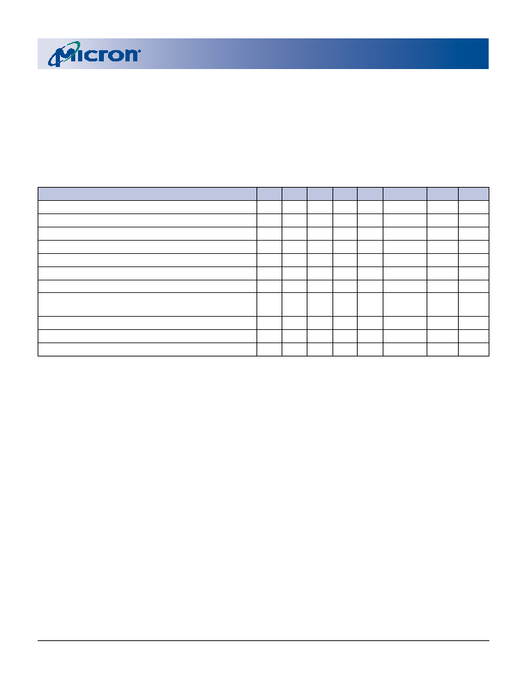
TRUTH TABLE 1 – COMMANDS AND DQM OPERATION
(Note: 1)
NAME (FUNCTION)
CS# RAS# CAS# WE# DQM
ADDR
DQs
NOTES
COMMAND INHIBIT (NOP)
H
XXXX
X
NO OPERATION (NOP)
L
H
X
ACTIVE (Select bank and activate row)
L
H
X
Bank/Row
X
3
READ (Select bank and column, and start READ burst)
L
H
L
H
L/H8
Bank/Col
X
4
WRITE (Select bank and column, and start WRITE burst)
L
H
L
L/H8
Bank/Col
Valid
4
BURST TERMINATE
L
H
L
X
Active
PRECHARGE (Deactivate row in bank or banks)
L
H
L
X
Code
X
5
AUTO REFRESH or SELF REFRESH
L
H
X
6, 7
(Enter self refresh mode)
LOAD MODE REGISTER
L
X
Op-Code
X
2
Write Enable/Output Enable
––––L
–
Active
8
Write Inhibit/Output High-Z
––––
H
–
High-Z
8
following the Operation section; these tables provide
current state/next state information.
Commands
Truth Table 1 provides a quick reference of available
commands. This is followed by a written description of
each command. Three additional Truth Tables appear
NOTE: 1. CKE is HIGH for all commands shown except SELF REFRESH.
2. A0-A11 define the op-code written to the mode register.
3. A0-A11 provide row address, and BA0, BA1 determine which bank is made active.
4. A0-A9; A11 (x4); A0-A9 (x8); or A0-A8 (x16) provide column address; A10 HIGH enables the auto precharge feature
(nonpersistent), while A10 LOW disables the auto precharge feature; BA0, BA1 determine which bank is being read
from or written to.
5. A10 LOW: BA0, BA1 determine the bank being precharged. A10 HIGH: All banks precharged and BA0, BA1 are “Don’t
Care.”
6. This command is AUTO REFRESH if CKE is HIGH, SELF REFRESH if CKE is LOW.
7. Internal refresh counter controls row addressing; all inputs and I/Os are “Don’t Care” except for CKE.
8. Activates or deactivates the DQs during WRITEs (zero-clock delay) and READs (two-clock delay).
相關(guān)PDF資料 |
PDF描述 |
|---|---|
| MT49H8M36HU-33 | 8M X 36 DDR DRAM, 0.3 ns, PBGA144 |
| MT4C1024DJ-6L | 1M X 1 FAST PAGE DRAM, 60 ns, PDSO20 |
| MT4C2M8A1DJ-7STR | 2M X 8 FAST PAGE DRAM, 70 ns, PDSO28 |
| MT4LC1M16C5TG-8S | 1M X 16 FAST PAGE DRAM, 80 ns, PDSO44 |
| MT4LC2M8A1DJ-6TR | 2M X 8 FAST PAGE DRAM, 60 ns, PDSO28 |
相關(guān)代理商/技術(shù)參數(shù) |
參數(shù)描述 |
|---|
發(fā)布緊急采購,3分鐘左右您將得到回復(fù)。