- 您現(xiàn)在的位置:買賣IC網(wǎng) > PDF目錄371014 > MC145170 (Motorola, Inc.) PLL Frequency Synthesizer(PLL頻率發(fā)生器) PDF資料下載
參數(shù)資料
| 型號(hào): | MC145170 |
| 廠商: | Motorola, Inc. |
| 英文描述: | PLL Frequency Synthesizer(PLL頻率發(fā)生器) |
| 中文描述: | 鎖相環(huán)頻率合成器(PLL頻率發(fā)生器) |
| 文件頁(yè)數(shù): | 6/14頁(yè) |
| 文件大?。?/td> | 173K |
| 代理商: | MC145170 |
第1頁(yè)第2頁(yè)第3頁(yè)第4頁(yè)第5頁(yè)當(dāng)前第6頁(yè)第7頁(yè)第8頁(yè)第9頁(yè)第10頁(yè)第11頁(yè)第12頁(yè)第13頁(yè)第14頁(yè)

6
MOTOROLA RF/IF APPLICATIONS INFORMATION
capacitor C1. R1 is arbitrarily set to 1e99 and is not an active
part of the circuit however it must be included to prevent open
pin errors from the PSpice software. The GVALUE function is
used to perform the generation of v(int). There is some
interaction between the integrator, (GVALUE output and C1)
and R1. V(int) is a continuous ramp that is loaded by the
resistance of R1. Unless the GVALUE output current is
sufficiently large for the value chosen for R1, the VCO control
voltage required to maintain lock will increase throughout the
simulation producing nonlinear operation. Modifications to
the circuit can be performed either by changing the values in
the parameter list or for major changes to the VCO
characteristics, the equations for the sin generator or control
voltage can be altered.
The output of the sine generator is amplified by 1000 to
produce a sharp rise/fall time and the output limited to swing
between the values of zero volts and +5 volts to convert it to
a digital output. The resultant circuit/symbol accepts a
voltage input from the loop filter and produces a square wave
output at the desired frequency. This frequency should be
chosen to represent the frequency present at the output of
the N counter within the MC145170.
The second output represented by the ABM function is a
sine wave output of the frequency expected from the actual
VCO. The primary purpose of this output is to allow full
frequency simulation for spectrum analysis. By running a
transient analysis of sufficient time, it is possible to determine
spur content and level. If sufficient resolution is used in the
simulation, the PSpice probe FFT transform can be used to
provide the typical spectrum analyzer display.
Example
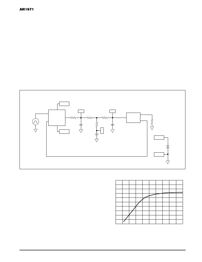
Design a PLL frequency synthesizer circuit to generate an
output stepping from 10 MHz to 12 MHz in 100 KHz
increments. In this example, (Figure 11), with an output
frequency of 10 MHz, N is chosen to be 100 and V2 is set for
a step frequency of 100 KHz. The loop filter is (B) shown in
the Phase–Locked Loop–Low Pass Filter Design section of
the MC145170 data sheet. The series resistance has been
split and Cc (C3 in Figure 11), inserted and additional filtering
(C1, R1), added.
Figure 11.
HB2
PWR
GND
PDout
Ref
In
HB1
GND
PWR
R3
10 k
R4
10 k
R1
10 k
820 p
R5
0
0
C2
C3
0
10 nF
GND
PWR
V1
5 V
+
–
0
50
R2
Ctrl
0
+
–
+
+
+
IC=
IC=
390 pF
0
C1
V2
Out
VCOout
IC=
12 k
The performance of the VCO chosen for this application is
shown in Figure 12. The VCO gain may be obtained from the
relationship between the delta of fVCO and the delta of vVCO
at the nominal operating frequency. Limiting operation to
below 15 MHz will keep the gain linear enough to fit the
model. If the output is to be operated at near 10 MHz, from
the graph
KVCO = 2*PI*delta(fVCO)/delta(vVCO) = 1.27e7 rad/sec/V
The phase detector gain is given by the MC145170 data
sheet as
Kphi = VDD/4*PI volts per radian for PDout.
Letting
wn = 2*PI*fR/50 = 12,566 rad/s
the loop filter values can be calculated. Choosing C = 10 nf,
the value for R1+R2 can be calculated.
(R1+R2) = Kphi*KVCO/N*C*(wn)2 ~ 32k
0
2
4
6
8
10
Vin, INPUT VOLTAGE (VOLTS)
Figure 12.
,
f
18
16
14
12
10
8
For a damping factor of 0.8,
R2 = (0.8/0.5*wn - N/Kphi*KVCO)/C ~ 12k
發(fā)布緊急采購(gòu),3分鐘左右您將得到回復(fù)。