- 您現(xiàn)在的位置:買賣IC網(wǎng) > PDF目錄377895 > MB86967PFV (FUJITSU LTD) LAN Controller with PC Card, ISA Bus, and General-purpose Bus Interfaces PDF資料下載
參數(shù)資料
| 型號: | MB86967PFV |
| 廠商: | FUJITSU LTD |
| 元件分類: | 微控制器/微處理器 |
| 英文描述: | LAN Controller with PC Card, ISA Bus, and General-purpose Bus Interfaces |
| 中文描述: | 1 CHANNEL(S), 10M bps, LOCAL AREA NETWORK CONTROLLER, PQFP80 |
| 封裝: | PLASTIC, LQFP-80 |
| 文件頁數(shù): | 45/129頁 |
| 文件大小: | 1499K |
| 代理商: | MB86967PFV |
第1頁第2頁第3頁第4頁第5頁第6頁第7頁第8頁第9頁第10頁第11頁第12頁第13頁第14頁第15頁第16頁第17頁第18頁第19頁第20頁第21頁第22頁第23頁第24頁第25頁第26頁第27頁第28頁第29頁第30頁第31頁第32頁第33頁第34頁第35頁第36頁第37頁第38頁第39頁第40頁第41頁第42頁第43頁第44頁當(dāng)前第45頁第46頁第47頁第48頁第49頁第50頁第51頁第52頁第53頁第54頁第55頁第56頁第57頁第58頁第59頁第60頁第61頁第62頁第63頁第64頁第65頁第66頁第67頁第68頁第69頁第70頁第71頁第72頁第73頁第74頁第75頁第76頁第77頁第78頁第79頁第80頁第81頁第82頁第83頁第84頁第85頁第86頁第87頁第88頁第89頁第90頁第91頁第92頁第93頁第94頁第95頁第96頁第97頁第98頁第99頁第100頁第101頁第102頁第103頁第104頁第105頁第106頁第107頁第108頁第109頁第110頁第111頁第112頁第113頁第114頁第115頁第116頁第117頁第118頁第119頁第120頁第121頁第122頁第123頁第124頁第125頁第126頁第127頁第128頁第129頁
45
MB86967
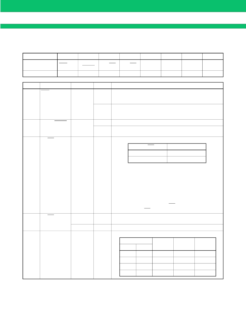
(7) DLCR6: Control Register 1
DLCR6 sets the MB86966 operation modes.
(Continued)
* :This register is accessible only for the device initialization.
Bit 7
Bit 6
100NS/
150NS
0
Bit 5
Bit 4
Bit 3
TX BUF
SIZE 1
0
Bit 2
TX BUF
SIZE 0
1
Bit 1
BUF
SIZE 1
1
Bit 0
BUF
SIZE 0
0
Read/Write
ENA DLC
SB/SW
BB/BW
Initial Value
1
1
1
Bit no.
7
Bit name
ENA DLC
(Enable Data
Link Controller)
Operation
Read/Write
Value
0
Function
When 0 is written to this bit, the MB86967 is ready for
transmitting and receiving. When this bit is 0, the node ID
register and multicast address register cannot be accessed.
The data link controller and buffer manager in the MB86967
are initialized and both the transmitter and receiver buffers are
also initialized.
Sets cycle time of external SRAM to 150 ns
Sets cycle time of external SRAM to 100 ns.
In this case, use SRAM with an access time of 80 ns or less.
Selects width of system data bus
1
6
100NS/150NS
(SRAM Cycle
Time Select)
Read/Write
0
1
5
SB/SW
(System Bus
Width Select)
Read/Write
—
PC Card Mode
When 1 is written to bit 5 (IOIS8) of the CCR1, the SB/-SW
bit is set to 1, placing the system data bus in the byte
transfer mode. When 0 is written, the SB/-SW bit is set to 0,
placing the system data bus in the word transfer mode.
In the PC card mode, writing to the SB/-SW bit is performed
by CCR1. Writing from DLCR6 does not affect bit 5.
General-purpose Bus Mode
The reversed value of the SB/SW bit is output to the
external pin SB/SW.
The width of the buffer memory data bus is fixed to 8 bits. The
read value of this bit is always 1.
Not affected
Sets size of transmitter buffer.
4
BB/BW
(Buffer Memory
Bus Width)
Read
1
Write
—
—
3 and 2 TX BUF SIZE 1
TX BUF SIZE 0
(Transmitter
Buffer Size)
Read/Write
SB/SW
0
1
System Data Bus
16 bit
8 bit
TX BUF SIZE
1
0
0
1
1
Bank
Capacity
Bank
Count
Buffer
Capacity
0
0
1
0
1
2 Kbyte
2 Kbyte
4 Kbyte
8 Kbyte
1
2
2
2
2 Kbyte
4 Kbyte
8 Kbyte
16 Kbyte
相關(guān)PDF資料 |
PDF描述 |
|---|---|
| MB86977 | IP PACKET FORWARDING ENGINE |
| MB86977PFV-G-BND | IP PACKET FORWARDING ENGINE |
| MB86H20 | SmartMPEG |
| MB86H21 | MPEG-2 Decoder with Integrated NDS ICAM |
| MB86H22 | MPEG-2 Decoder for ext. Temperature Range |
相關(guān)代理商/技術(shù)參數(shù) |
參數(shù)描述 |
|---|---|
| MB86977 | 制造商:FUJITSU 制造商全稱:Fujitsu Component Limited. 功能描述:IP PACKET FORWARDING ENGINE |
| MB86977PFV-G-BND | 制造商:FUJITSU 制造商全稱:Fujitsu Component Limited. 功能描述:IP PACKET FORWARDING ENGINE |
| MB86A21PMC-G-BNDE1 | 制造商:FUJITSU 功能描述: |
| MB86A21PMC-G-JNE1 | 制造商:FUJITSU 功能描述: |
| MB86A22PMC-ES-BNDE1 | 制造商:FUJITSU 功能描述: |
發(fā)布緊急采購,3分鐘左右您將得到回復(fù)。