- 您現(xiàn)在的位置:買賣IC網(wǎng) > PDF目錄377549 > IS42S16128-10T (INTEGRATED SILICON SOLUTION INC) 128K Words x 16 Bits x 2 Banks (4-MBIT) SYNCHRONOUS DYNAMIC RAM PDF資料下載
參數(shù)資料
| 型號(hào): | IS42S16128-10T |
| 廠商: | INTEGRATED SILICON SOLUTION INC |
| 元件分類: | DRAM |
| 英文描述: | 128K Words x 16 Bits x 2 Banks (4-MBIT) SYNCHRONOUS DYNAMIC RAM |
| 中文描述: | 256K X 16 SYNCHRONOUS DRAM, 10 ns, PDSO50 |
| 封裝: | 0.400 INCH, TSOP2-50 |
| 文件頁(yè)數(shù): | 22/75頁(yè) |
| 文件大小: | 638K |
| 代理商: | IS42S16128-10T |
第1頁(yè)第2頁(yè)第3頁(yè)第4頁(yè)第5頁(yè)第6頁(yè)第7頁(yè)第8頁(yè)第9頁(yè)第10頁(yè)第11頁(yè)第12頁(yè)第13頁(yè)第14頁(yè)第15頁(yè)第16頁(yè)第17頁(yè)第18頁(yè)第19頁(yè)第20頁(yè)第21頁(yè)當(dāng)前第22頁(yè)第23頁(yè)第24頁(yè)第25頁(yè)第26頁(yè)第27頁(yè)第28頁(yè)第29頁(yè)第30頁(yè)第31頁(yè)第32頁(yè)第33頁(yè)第34頁(yè)第35頁(yè)第36頁(yè)第37頁(yè)第38頁(yè)第39頁(yè)第40頁(yè)第41頁(yè)第42頁(yè)第43頁(yè)第44頁(yè)第45頁(yè)第46頁(yè)第47頁(yè)第48頁(yè)第49頁(yè)第50頁(yè)第51頁(yè)第52頁(yè)第53頁(yè)第54頁(yè)第55頁(yè)第56頁(yè)第57頁(yè)第58頁(yè)第59頁(yè)第60頁(yè)第61頁(yè)第62頁(yè)第63頁(yè)第64頁(yè)第65頁(yè)第66頁(yè)第67頁(yè)第68頁(yè)第69頁(yè)第70頁(yè)第71頁(yè)第72頁(yè)第73頁(yè)第74頁(yè)第75頁(yè)
22
Integrated Silicon Solution, Inc. — 1-800-379-4774
Rev. A
03/13/00
IS42S16128
ISSI
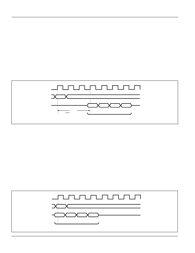
Burst Read
The read cycle is started by executing the read command.
The address provided during read command execution is
used as the starting address. First, the data correspond-
ing to this address is output in synchronization with the
clock signal after the
CAS
latency period. Next, data
corresponding to an address generated automatically by
the device is output in synchronization with the clock
signal.
The output buffers go to the LOW impedance state
CAS
latency minus one cycle after the read command, and go
to the HIGH impedance state automatically after the last
data is output. However, the case where the burst length
is a full page is an exception. In this case the output
buffers must be set to the high impedance state by
executing a burst stop command.
Note that upper byte and lower byte output data can be
masked independently under control of the signals ap-
plied to the U/LDQM pins. The delay period (t
QMD
) is fixed
at two, regardless of the
CAS
latency setting, when this
function is used.
The selected bank must be set to the active state before
executing this command.
BURST LENGTH
CAS LATENCY
t
CAC
READ
COMMAND
I/O
CLK
D
OUT
0
D
OUT
1
D
OUT
2
D
OUT
3
CAS
latency = 3, burst length = 4
Burst Write
The write cycle is started by executing the command. The
address provided during write command execution is
used as the starting address, and at the same time, data
for this address is input in synchronization with the clock
signal.
Next, data is input in other in synchronization with the
clock signal. During this operation, data is written to
address generated automatically by the device. This
cycle terminates automatically after a number of clock
cycles determined by the stipulated burst length. How-
ever, the case where the burst length is a full page is an
exception. In this case the write cycle must be terminated
by executing a burst stop command.
The latency for I/O pin data input is zero, regardless of the
CAS
latency setting. However, a wait period (write recov-
ery: t
DPL
) after the last data input is required for the device
to complete the write operation.
Note that the upper byte and lower byte input data can be
masked independently under control of the signals ap-
plied to the U/LDQM pins. The delay period (t
DMD
) is fixed
at zero, regardless of the
CAS
latency setting, when this
function is used.
The selected bank must be set to the active state before
executing this command.
BURST LENGTH
WRITE
COMMAND
I/O
CLK
D
IN
0
D
IN
1
D
IN
2
D
IN
3
CAS
latency = 2,3, burst length = 4
相關(guān)PDF資料 |
PDF描述 |
|---|---|
| IS42S16128-12T | 128K Words x 16 Bits x 2 Banks (4-MBIT) SYNCHRONOUS DYNAMIC RAM |
| IS42S16128-8T | Chassis Mount and Din Rail Filters RoHS Compliant: Yes |
| IS42S16160B-7TL | 32Meg x 8, 16Meg x16 256-MBIT SYNCHRONOUS DRAM |
| IS42S16160B-7TLI | 32Meg x 8, 16Meg x16 256-MBIT SYNCHRONOUS DRAM |
| IS42S83200B | 32Meg x 8, 16Meg x16 256-MBIT SYNCHRONOUS DRAM |
相關(guān)代理商/技術(shù)參數(shù) |
參數(shù)描述 |
|---|---|
| IS42S16128-12T | 制造商:ISSI 制造商全稱:Integrated Silicon Solution, Inc 功能描述:128K Words x 16 Bits x 2 Banks (4-MBIT) SYNCHRONOUS DYNAMIC RAM |
| IS42S16128-8T | 制造商:ISSI 制造商全稱:Integrated Silicon Solution, Inc 功能描述:128K Words x 16 Bits x 2 Banks (4-MBIT) SYNCHRONOUS DYNAMIC RAM |
| IS42S16160A-6T | 制造商:ISSI 制造商全稱:Integrated Silicon Solution, Inc 功能描述:256 Mb Synchronous DRAM |
| IS42S16160A-6TL | 制造商:ISSI 制造商全稱:Integrated Silicon Solution, Inc 功能描述:256 Mb Synchronous DRAM |
| IS42S16160A-7T | 制造商:Integrated Silicon Solution Inc 功能描述: |
發(fā)布緊急采購(gòu),3分鐘左右您將得到回復(fù)。