- 您現(xiàn)在的位置:買賣IC網(wǎng) > PDF目錄379203 > IBM025170 (IBM Microeletronics) 4Mb(256K X 16) MULTIPORT VIDEO RAM(4M位(256K X 16)多端口視頻RAM) PDF資料下載
參數(shù)資料
| 型號: | IBM025170 |
| 廠商: | IBM Microeletronics |
| 英文描述: | 4Mb(256K X 16) MULTIPORT VIDEO RAM(4M位(256K X 16)多端口視頻RAM) |
| 中文描述: | 4Mb的(256 × 16)多端口視頻內(nèi)存(4分位(256 × 16)多端口視頻內(nèi)存) |
| 文件頁數(shù): | 10/65頁 |
| 文件大小: | 841K |
| 代理商: | IBM025170 |
第1頁第2頁第3頁第4頁第5頁第6頁第7頁第8頁第9頁當(dāng)前第10頁第11頁第12頁第13頁第14頁第15頁第16頁第17頁第18頁第19頁第20頁第21頁第22頁第23頁第24頁第25頁第26頁第27頁第28頁第29頁第30頁第31頁第32頁第33頁第34頁第35頁第36頁第37頁第38頁第39頁第40頁第41頁第42頁第43頁第44頁第45頁第46頁第47頁第48頁第49頁第50頁第51頁第52頁第53頁第54頁第55頁第56頁第57頁第58頁第59頁第60頁第61頁第62頁第63頁第64頁第65頁
IBM025170
IBM025171
256K X 16 MULTIPORT VIDEO RAM
IBM025160
IBM025161
IBM Corporation, 1995. All rights reserved.
Use is further subject to the provisions at the end of this document.
Page 10 of 65
33G0307
SA14-4751-05
Revised 3/98
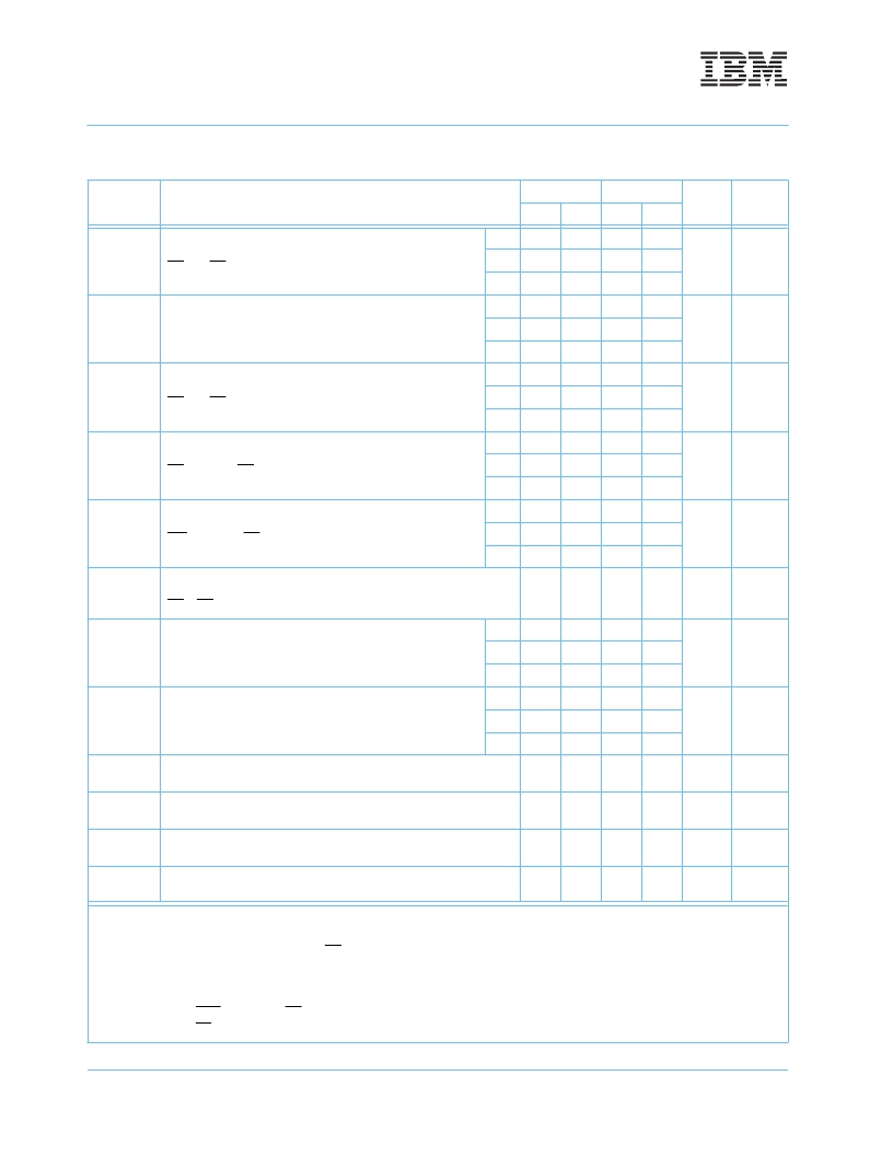
DC Electrical Characteristics
(T
A
= 0 to +70
°
C, V
CC
= 3.3V
±
0.3V or V
CC
= 5.0V
±
0.5V)
Symbol
Parameter
5.0 Volt
3.3 Volt
Units
Notes
Min.
Max.
Min.
Max.
I
CC1
Operating Current (Random)
Average Power Supply Operating Current
(RE and CE Cycling, t
RC
=120ns for -60 and -6H, t
RC
=130ns
for -70, SC = 0)
-6H
—
135
—
135
mA
1, 2, 3, 6
-60
—
135
—
135
-70
—
130
—
130
I
CC2
Operating Current (Serial)
Average Power Supply Current
(t
SCC
= 20ns for -60 and -6H, t
SCC
= 23ns for -70)
-6H
—
40
—
40
mA
1, 2, 7
-60
—
40
—
40
-70
—
35
—
35
I
CC3
Operating Current (Both Port)
Average Power Supply Current
(RE and CE Cycling, t
RC
=120ns & t
SCC
= 20ns for -60 and -
6H, t
RC
=130ns & t
SCC
= 23ns for -70)
-6H
—
160
—
160
mA
1, 2, 3,
6, 7
-60
—
160
—
16 0
-70
—
150
—
150
I
CC4
Fast Page Mode Current
Average Power Supply Current, Fast Page Mode
(RE V
IL
Min., CE Cycling, t
PC
= 40ns for -60 and -6H,
t
PC
=45ns for -70)
-6H
—
80
—
80
mA
1, 2, 4,
6, 7
-60
—
80
—
80
-70
—
70
—
70
I
CC5
Fast Page Mode Current (Serial)
Average Power Supply Current, Fast Page/Serial
(RE
≤
V
IL
Min., CE Cycling, t
PC
= 40ns & t
SCC
= 20ns for -60
and -6H, t
PC
= 45ns & t
SCC
= 23ns for -70)
-6H
—
85
—
85
mA
1, 2, 7
-60
—
85
—
85
-70
—
75
—
75
I
CC6
Standby Supply Current
Power Supply Standby Current
(RE = CE = VCC, SC = 0V)
—
5
—
5
mA
I
CC7
Data Transfer Current
Average Power Supply Current
(t
RC
=120ns for -60 and -6H, t
RC
= 130ns for -70, SC = 0V)
-6H
—
130
—
130
mA
-60
—
130
—
130
-70
—
120
—
120
I
CC8
Data Transfer Current
Average Power Supply Current
(t
SCC
= 20ns for -60 and -6H, t
SCC
= 23ns for -70)
-6H
—
140
—
140
mA
-60
—
140
—
140
-70
—
130
—
130
I
I(L)
Input Leakage Current, any input
(0.0
≤
V
IN
≤
(V
CC
+ 1.0V)), All Other Pins Not Under Test = 0V
-10
+10
-10
10
μ
A
I
O(L)
Output Leakage Current
(D
OUT
is disabled, 0.0
≤
V
OUT
≤
V
CC
(max))
-10
+10
-10
10
μ
A
V
OH
Output Level (TTL)
Output “H” Level Voltage (I
OUT
= -1mA, Random and Serial)
2.4
—
2.4
—
V
4
V
OL
Output Level (TTL)
Output “L” Level Voltage (I
OUT
= +2.0mA, Random and Serial)
—
0.4
—
0.4
V
4
1. I
CC1
, I
CC2
, I
CC3
, I
CC4
, I
CC5
, I
CC7
and I
CC8
depend on cycle rate.
2. I
CC1
, I
CC2
, I
CC3
, I
CC4
, I
CC5
, I
CC7
and I
CC8
depend on output loading. Specified values are obtained with the output open.
3. Measured with one address change per RE cycle.
4. Measured with one column address change per page cycle.
5. V
IH
(min.) and V
IL
(max.) are reference levels for measuring timing of input signals. Also, transition times are measured between V
IH
and V
IL
.
6. Measured with TRG = V
IH
when CE = V
IL
.
7. Measured with SE = V
IH
.
相關(guān)PDF資料 |
PDF描述 |
|---|---|
| IBM025171 | 4Mb(256K X 16) MULTIPORT VIDEO RAM(4M位(256K X 16)多端口視頻RAM) |
| IBM038329NL6B | 256K x 32 Synchronous Graphics RAM(256K x 32 高性能8M位CMOS同步動態(tài)RAM(帶內(nèi)置的圖形性能)) |
| IBM038329NP6B | 256K x 32 Synchronous Graphics RAM(256K x 32 高性能8M位CMOS同步動態(tài)RAM(帶內(nèi)置的圖形性能)) |
| IBM041812PQKB | 64K X 18 BURST SRAM(64K X 18高性能可猝發(fā)同步CMOS靜態(tài)RAM) |
| IBM041813PPLB | 64K X 18 BURST PIPELINE SRAM(1M (64K X 18)同步可猝發(fā)流水線式線式高性能靜態(tài)RAM) |
相關(guān)代理商/技術(shù)參數(shù) |
參數(shù)描述 |
|---|---|
| IBM02N6153 | 制造商:AVED Memory Products 功能描述: |
| IBM02N7991 | 制造商:AVED Memory Products 功能描述: |
| IBM02N7994 | 制造商:AVED Memory Products 功能描述: |
| IBM0312164PT3A360 | 制造商:IBM 功能描述:* |
| IBM0312404CT3A260 | 制造商:IBM 功能描述:* |
發(fā)布緊急采購,3分鐘左右您將得到回復(fù)。