- 您現(xiàn)在的位置:買賣IC網(wǎng) > PDF目錄383075 > HSP50214BVI (HARRIS SEMICONDUCTOR) Programmable Downconverter PDF資料下載
參數(shù)資料
| 型號(hào): | HSP50214BVI |
| 廠商: | HARRIS SEMICONDUCTOR |
| 元件分類: | 通信及網(wǎng)絡(luò) |
| 英文描述: | Programmable Downconverter |
| 中文描述: | SPECIALTY TELECOM CIRCUIT, PQFP120 |
| 文件頁(yè)數(shù): | 17/60頁(yè) |
| 文件大?。?/td> | 573K |
| 代理商: | HSP50214BVI |
第1頁(yè)第2頁(yè)第3頁(yè)第4頁(yè)第5頁(yè)第6頁(yè)第7頁(yè)第8頁(yè)第9頁(yè)第10頁(yè)第11頁(yè)第12頁(yè)第13頁(yè)第14頁(yè)第15頁(yè)第16頁(yè)當(dāng)前第17頁(yè)第18頁(yè)第19頁(yè)第20頁(yè)第21頁(yè)第22頁(yè)第23頁(yè)第24頁(yè)第25頁(yè)第26頁(yè)第27頁(yè)第28頁(yè)第29頁(yè)第30頁(yè)第31頁(yè)第32頁(yè)第33頁(yè)第34頁(yè)第35頁(yè)第36頁(yè)第37頁(yè)第38頁(yè)第39頁(yè)第40頁(yè)第41頁(yè)第42頁(yè)第43頁(yè)第44頁(yè)第45頁(yè)第46頁(yè)第47頁(yè)第48頁(yè)第49頁(yè)第50頁(yè)第51頁(yè)第52頁(yè)第53頁(yè)第54頁(yè)第55頁(yè)第56頁(yè)第57頁(yè)第58頁(yè)第59頁(yè)第60頁(yè)
3-17
For 12 bits, Equation 7 becomes:
For 10 bits, Equation 7 becomes:
For 8 bits, Equation 7 becomes:
Figure 15 is a plot of Equations 8A through 8D. The 4-bit CIC
Shift Gain word has a range from 0 to 15. The 6-bit
Decimation Factor counter preload field, (R-1), has a range
from 0 to 63, limited by the input resolution as cited above.
Using the Input Gain Adjust Control Signals
The input gain offset control GAINADJ(2:0)) is provided to
offset the signal gain through the part, i.e., to keep the CIC
filter output level constant as the analog front end
attenuation is changed. The gain adjust offset is 6dB per
code, so the gain adjust range is 0 to 42dB. For example, if
12dB of attenuation is switched in at the receiver RF front
end, a code of 2 would increase the gain at the input to the
CIC filter up 12dB so that the CIC filter output would not drop
by 12dB. This fixed gain adjust eliminates the need for the
software to continually normalize.
One must exercise care when using this function as it can
cause overflow in the CIC filter. Each gain adjust in the
shifter from the gain adjust control signals is the equivalent
of an extra bit of input. The maximum decimation in the CIC
is reduced accordingly. With a decimation of 32, all 40 bits of
the CIC are needed, so no input offset gain is allowed. As
the decimation is reduced, the allowable offset gain
increases. Table 3 shows the decimation range versus
desired offset gain range. Table 3 assumes that the CIC Shift
Gain has been programmed per Equation 7 or 8A.
The CIC filter decimation counter can be loaded synchronous
with other PDC chips, using the SYNCIN1 signal and the CIC
External Sync Enable bit. The CIC external Sync Enable is set
via Control Word 0, Bit 19.
Halfband Decimating Filters
The Programmable Down Converter has five halfband filter
stages, as shown in Figure 17. Each stage decimates by 2
and filters out half of the available bandwidth. The first
halfband, or HB1, has 7 taps. The remaining halfbands;
HB2, HB3, HB4, and HB5; have 11, 15, 19, and 23 taps
respectively. The coefficients for these halfbands are given in
Table 4. Figure 18 shows the frequency response of each of
the halfband filters with respect to normalized frequency, F
N
.
Frequency normalization is with respect to the input
sampling frequency of each filter section. Each stage is
activated by their respective bit location (15-20) in Control
Word 7. Any combination of halfband filters may be used, or
all may be bypassed.
Since each halfband filter section decimates by 2, the total
decimation through the halfband filter is given by:
where N = Number of Halfband Filters Selected (1 - 5).
SG
FLOOR 27
15
log
2
R
( )
5
]
for 5 < R < 40
for 4
–
=
=
(EQ. 8B)
R
5
≤
≤
SG
FLOOR 29
15
log
2
R
( )
5
]
for 6 < R < 52
for 4
–
=
=
(EQ. 8C)
R
6
≤
≤
SG
FLOOR 31
log
2
R
( )
5
]
for 9 < R < 64
for 4
–
=
(EQ. 8D)
15
=
R
9
≤
≤
C
2
-18
2
-19
2
-20
2
-21
2
-22
2
-23
2
-24
2
-25
2
-26
2
-27
2
-28
2
-29
2
-30
2
-31
2
-32
2
-33
2
-34
2
-35
2
-36
2
-37
2
-38
2
-39
2
-4
2
-5
2
-6
2
-7
2
-8
2
-9
2
-10
2
-11
2
-12
2
-13
2
-14
2
-15
2
-16
2
-17
2
-1
2
-2
2
-3
0
A
2
-4
2
-5
2
-6
2
-7
2
-8
2
-9
2
-10
2
-11
2
-12
2
-13
2
-14
2
-1
2
-2
2
-3
0
I
2
-4
2
-5
2
-6
2
-7
2
-8
2
-9
2
-10
2
-11
2
-12
2
-13
2
-14
2
-1
2
-2
2
-3
0
I
2
-18
2
-19
2
-20
2
-21
2
-22
2
-23
2
-24
2
-25
2
-26
2
-27
2
-28
2
-29
2
-30
2
-31
2
-32
2
-33
2
-34
2
-35
2
-4
2
-5
2
-6
2
-7
2
-8
2
-9
2
-10
2
-11
2
-12
2
-13
2
-14
2
-15
2
-16
2
-17
2
-1
2
-2
2
-3
0
2
-18
2
-19
2
-20
2
-21
2
-22
2
-23
2
-24
2
-25
2
-26
2
-27
2
-28
2
-29
2
-30
2
-31
2
-4
2
-5
2
-6
2
-7
2
-8
2
-9
2
-10
2
-11
2
-12
2
-13
2
-14
2
-15
2
-16
2
-17
2
-1
2
-2
2
-3
0
2
-18
2
-19
2
-20
2
-21
2
-22
2
-23
2
-24
2
-25
2
-26
2
-27
2
-28
2
-29
2
-30
2
-31
2
-4
2
-5
2
-6
2
-7
2
-8
2
-9
2
-10
2
-11
2
-12
2
-13
2
-14
2
-15
2
-16
2
-17
2
-1
2
-2
2
-3
0
2
-18
2
-19
2
-20
2
-21
2
-22
2
-23
2
-24
2
-25
2
-26
2
-27
2
-28
2
-29
2
-30
2
-31
2
-4
2
-5
2
-6
2
-7
2
-8
2
-9
2
-10
2
-11
2
-12
2
-13
2
-14
2
-15
2
-16
2
-17
2
-1
2
-2
2
-3
0
2
-18
2
-19
2
-20
2
-21
2
-22
2
-23
2
-4
2
-5
2
-6
2
-7
2
-8
2
-9
2
-10
2
-11
2
-12
2
-13
2
-14
2
-15
2
-16
2
-17
2
-1
2
-2
2
-3
0
A
A
A
A
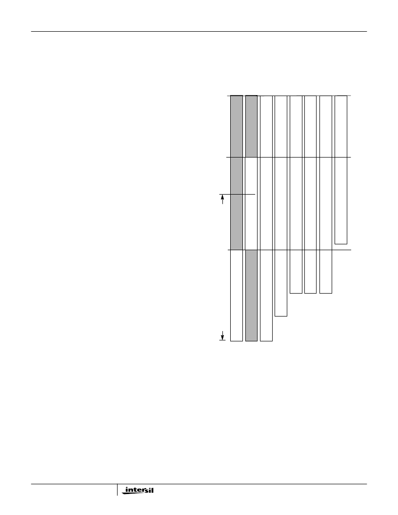
FIGURE 16. CIC FILTER BIT WEIGHTING
O
(
(
O
NOTE: If 14 input bits are not needed, the gain adjust can be in-
creased by one for each bit that the input is shifted down
at the input. For example, if only 12 bits are needed, an
offset range of 24dB is possible for a decimation of 24.
DEC
HB
2
N
=
(EQ. 9)
HSP50214B
相關(guān)PDF資料 |
PDF描述 |
|---|---|
| HT84 | ADSL Coupling Transformers |
| HT84-00594 | ADSL Coupling Transformers |
| HT8400594S | ADSL Coupling Transformers |
| HT84-00595 | ADSL Coupling Transformers |
| HT84-00596 | ADSL Coupling Transformers |
相關(guān)代理商/技術(shù)參數(shù) |
參數(shù)描述 |
|---|---|
| HSP50214BVIZ | 功能描述:上下轉(zhuǎn)換器 120L MQFP INDTEMP 14-BIT PROG DWNCNVRT RoHS:否 制造商:Texas Instruments 產(chǎn)品:Down Converters 射頻:52 MHz to 78 MHz 中頻:300 MHz LO頻率: 功率增益: P1dB: 工作電源電壓:1.8 V, 3.3 V 工作電源電流:120 mA 最大功率耗散:1 W 最大工作溫度:+ 85 C 安裝風(fēng)格:SMD/SMT 封裝 / 箱體:PQFP-128 |
| HSP50214VC | 制造商:Rochester Electronics LLC 功能描述:- Bulk |
| HSP50214VI | 制造商:Rochester Electronics LLC 功能描述:- Bulk |
| HSP50215 | 制造商:INTERSIL 制造商全稱:Intersil Corporation 功能描述:DSP Modulator Evaluation Board |
| HSP50215EVAL | 制造商:INTERSIL 制造商全稱:Intersil Corporation 功能描述:DSP Modulator Evaluation Board |
發(fā)布緊急采購(gòu),3分鐘左右您將得到回復(fù)。