- 您現(xiàn)在的位置:買賣IC網(wǎng) > PDF目錄383075 > HSP50214AVC (HARRIS SEMICONDUCTOR) Programmable Downconverter PDF資料下載
參數(shù)資料
| 型號(hào): | HSP50214AVC |
| 廠商: | HARRIS SEMICONDUCTOR |
| 元件分類: | 通信及網(wǎng)絡(luò) |
| 英文描述: | Programmable Downconverter |
| 中文描述: | SPECIALTY TELECOM CIRCUIT, PQFP120 |
| 文件頁(yè)數(shù): | 46/60頁(yè) |
| 文件大小: | 467K |
| 代理商: | HSP50214AVC |
第1頁(yè)第2頁(yè)第3頁(yè)第4頁(yè)第5頁(yè)第6頁(yè)第7頁(yè)第8頁(yè)第9頁(yè)第10頁(yè)第11頁(yè)第12頁(yè)第13頁(yè)第14頁(yè)第15頁(yè)第16頁(yè)第17頁(yè)第18頁(yè)第19頁(yè)第20頁(yè)第21頁(yè)第22頁(yè)第23頁(yè)第24頁(yè)第25頁(yè)第26頁(yè)第27頁(yè)第28頁(yè)第29頁(yè)第30頁(yè)第31頁(yè)第32頁(yè)第33頁(yè)第34頁(yè)第35頁(yè)第36頁(yè)第37頁(yè)第38頁(yè)第39頁(yè)第40頁(yè)第41頁(yè)第42頁(yè)第43頁(yè)第44頁(yè)第45頁(yè)當(dāng)前第46頁(yè)第47頁(yè)第48頁(yè)第49頁(yè)第50頁(yè)第51頁(yè)第52頁(yè)第53頁(yè)第54頁(yè)第55頁(yè)第56頁(yè)第57頁(yè)第58頁(yè)第59頁(yè)第60頁(yè)
46
Configuration Control Word Definitions
Note that in the Configuration Control Register Tables, some
of the available 32 bits in a Control Word are not used.
Unused bits do not need to be written to the Master Register.
If the destination only has 16 bits, then only 2 bytes need to be
written to the Master Register. Figure 45 details the timing for
proper operation of the Microprocessor Write Section. Bits
identified as “Reserved” should be programmed to a zero.
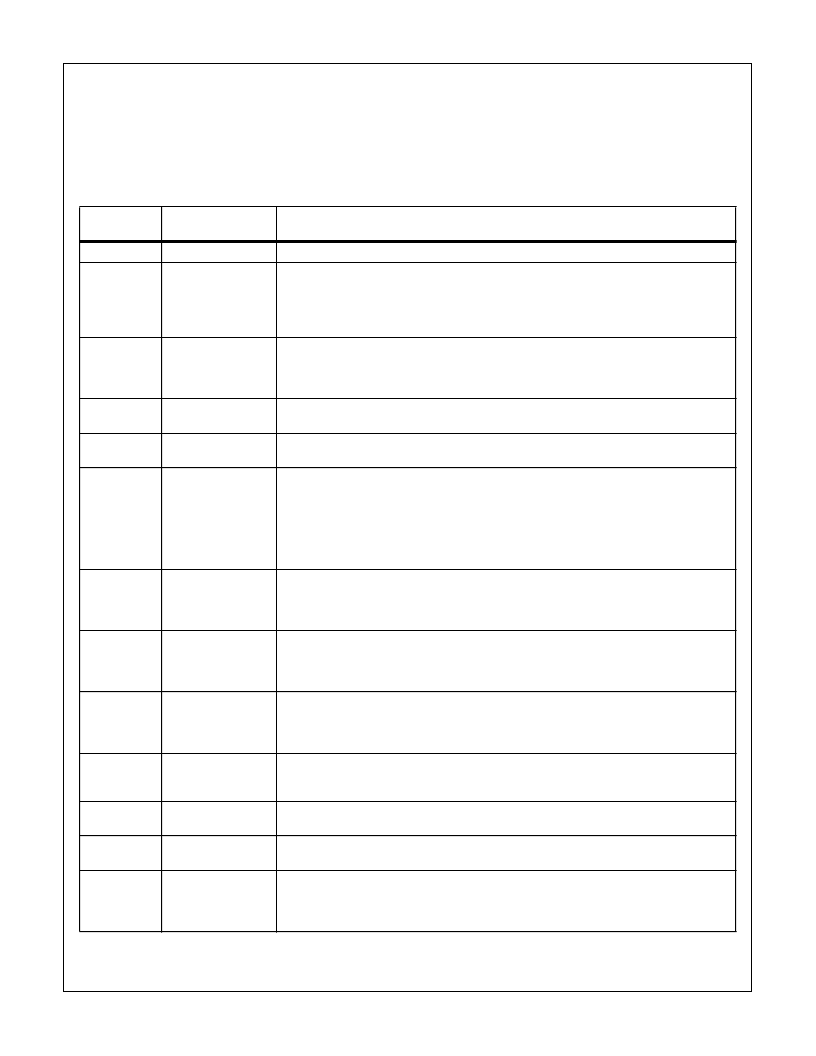
CONTROL WORD 0: CHIP CONFIGURATION, INPUT SECTION, CIC GAIN (SYNCHRONOUS TO CLKIN)
BIT
POSITION
FUNCTION
DESCRIPTION
31-21
Reserved
Reserved.
20
Carrier NCO External
Sync Enable
0- The SYNCIN1 pin has no effect on the Carrier NCO.
1- When the SYNCIN1 pin is asserted, the carrier center frequency and phase are updated from
the holding registers to the active register. Also, if bit 0 of this word is active, the carrier phase
accumulator feedback will be zeroed to set the Carrier NCO to a known phase, allowing the
NCOs of multiple parts to be initialized and updated synchronously.
19
CIC External Sync
Enable
0- The SYNCIN1 pin has no effect on the CIC filter.
1- When the SYNCIN1 pin is asserted, the decimation counter is loaded, allowing the decimation
counters in multiple chips to be synchronized. When CW27 bit-22 is set to a 1, SYNCIN1 will re-
set both front end and back end circuitry.
18
Input Format
0- Two’s Complement Input Format.
1- Offset Binary Input Format.
17
Input Mode
0- Input operates in Gated Mode.
1- Input operates in Interpolated Mode.
16-13
CIC Shift Gain
These bits control the barrel shifter at the input to the CIC filter. These bits are added to the
GAINADJ(2:0) pins to determine the total shift. The sum is saturated at 15. See the CIC Decima-
tion Filter Section for values to be programmed in this field based on CIC filter decimation. Bit 16
is the MSB.
SG = Floor [39 - (number of input bits) - 5log
2
(R)] for 4 < R < 31
SG = 15 for R = 4.
SG = 0 for R = 32.
12-7
CIC Decimation
Counter Preload
These bits control the decimation in the CIC filter. Program this field to R-1, where R is the de-
sired decimation factor in the filter. The decimation factor range is 4-32. See CIC Filter Section
for effective decimation factor range relative to the CIC Shift Gain value. Bit 12 is the MSB.
While this field allows values from 0 - 63, the valid values are in the range from 4- 32.
6
CIC Bypassed
Active high, this bit routes the output of the input shifter to the output of the CIC with no filtering.
When the CIC filter is bypassed, CLKIN must be at least twice the input sample rate (ENI should
be toggled to achieve this). When the CIC filter is bypassed, the bottom 24 bits of the barrel shifter
output are routed to the halfband filters.
5-4
Number of Offset
Frequency Bits
00 - 8 bits.
01 - 16.
10 - 24.
11 - 32.
3
Syncout CLK Select
This bit selects whether the SYNCOUT signal is generated from CLKIN of from PROCCLK
0- CLKIN.
1- PROCLK.
2
Clear Phase Accum
0- Enable accumulator in Carrier NCO.
1- Zero feedback in accumulator.
1
Carrier NCO Offset
Frequency Enable
When set to 1, this bit enables the offset frequency word to be added to the center frequency
Control Word. The offset is loaded serially via the COF and COFSYNC pins.
0
Carrier NCO Load
Phase Accum On
Update
When this bit is set to 1, the
μ
P update to the Carrier NCO frequency or an external carrier NCO
load using SYNCIN1 will zero the feedback of the phase accumulator, as well as update the
phase or frequency. This function can be used to set the NCO to a known phase synchronized
to an external event.
HSP50214A
相關(guān)PDF資料 |
PDF描述 |
|---|---|
| HSP50214AVI | Programmable Downconverter |
| HSP50214B | Programmable Downconverter |
| HSP50214BVC | Programmable Downconverter |
| HSP50214BVI | Programmable Downconverter |
| HT84 | ADSL Coupling Transformers |
相關(guān)代理商/技術(shù)參數(shù) |
參數(shù)描述 |
|---|---|
| HSP50214AVI | 制造商:INTERSIL 制造商全稱:Intersil Corporation 功能描述:Programmable Downconverter |
| HSP50214B | 制造商:INTERSIL 制造商全稱:Intersil Corporation 功能描述:Programmable Downconverter |
| HSP50214B_07 | 制造商:INTERSIL 制造商全稱:Intersil Corporation 功能描述:Programmable Downconverter |
| HSP50214BVC | 功能描述:上下轉(zhuǎn)換器 120L MQFP COMTEMP 14-BIT PROGRAMMABLE DOWNCONVERTER 65MSPS RoHS:否 制造商:Texas Instruments 產(chǎn)品:Down Converters 射頻:52 MHz to 78 MHz 中頻:300 MHz LO頻率: 功率增益: P1dB: 工作電源電壓:1.8 V, 3.3 V 工作電源電流:120 mA 最大功率耗散:1 W 最大工作溫度:+ 85 C 安裝風(fēng)格:SMD/SMT 封裝 / 箱體:PQFP-128 |
| HSP50214BVCZ | 功能描述:上下轉(zhuǎn)換器 120L MQFP COMTEMP 14-BIT PROG DWNCNVRT RoHS:否 制造商:Texas Instruments 產(chǎn)品:Down Converters 射頻:52 MHz to 78 MHz 中頻:300 MHz LO頻率: 功率增益: P1dB: 工作電源電壓:1.8 V, 3.3 V 工作電源電流:120 mA 最大功率耗散:1 W 最大工作溫度:+ 85 C 安裝風(fēng)格:SMD/SMT 封裝 / 箱體:PQFP-128 |
發(fā)布緊急采購(gòu),3分鐘左右您將得到回復(fù)。