- 您現(xiàn)在的位置:買賣IC網(wǎng) > PDF目錄383075 > HSP50214AVC (HARRIS SEMICONDUCTOR) Programmable Downconverter PDF資料下載
參數(shù)資料
| 型號: | HSP50214AVC |
| 廠商: | HARRIS SEMICONDUCTOR |
| 元件分類: | 通信及網(wǎng)絡(luò) |
| 英文描述: | Programmable Downconverter |
| 中文描述: | SPECIALTY TELECOM CIRCUIT, PQFP120 |
| 文件頁數(shù): | 12/60頁 |
| 文件大小: | 467K |
| 代理商: | HSP50214AVC |
第1頁第2頁第3頁第4頁第5頁第6頁第7頁第8頁第9頁第10頁第11頁當(dāng)前第12頁第13頁第14頁第15頁第16頁第17頁第18頁第19頁第20頁第21頁第22頁第23頁第24頁第25頁第26頁第27頁第28頁第29頁第30頁第31頁第32頁第33頁第34頁第35頁第36頁第37頁第38頁第39頁第40頁第41頁第42頁第43頁第44頁第45頁第46頁第47頁第48頁第49頁第50頁第51頁第52頁第53頁第54頁第55頁第56頁第57頁第58頁第59頁第60頁
12
The integration period counter can be set up to run continu-
ously or to count down and stop. Continuous integration
counter operation lets the counter run, with sampling occurring
every time the counter reaches zero. Because the processor
samples the detector read port asynchronous to the CLKIN,
data can be missed unless the status bit is monitored by the
processor to ensure that a sample is taken for every integration
count down sequence.
Additionally, in the HSP50214A, the ability to align the
start/restart of the input level detector integration period with an
external event is provided. This allows the sync signals, which
are synchronized to external events, to be used to align all of
the gain adjustments or measurements. If Control Word 27, Bit
17 is set to a logic one, the SYNCIN1 signal will cause the input
level detector to start/restart its integration period. If Control
Word 27, Bit 17 is set to a logic zero, control of the start/restart
of the input level detector integration period does not respond to
SYNCIN1.
In the count down and stop mode, the microprocessor read
commands can be synchronized to system events, such as the
start of a burst for a TDMA application. The integration counter
can be started at any time by writing to Control Word 2. At the
end of the integration period (counter = 0000), the upper 23 bits
of the accumulator are transferred to a holding register for read-
ing by the microprocessor. Note that it is not the restarting of
the counter (by writing to Control Word 2) that latches the cur-
rent value, but the end of the integration count. When the accu-
mulator results are latched, a bit is set in the Status Register to
notify the processor. Reading the most significant byte of the 23
bits clears the status bit. See the Microprocessor Read Section.
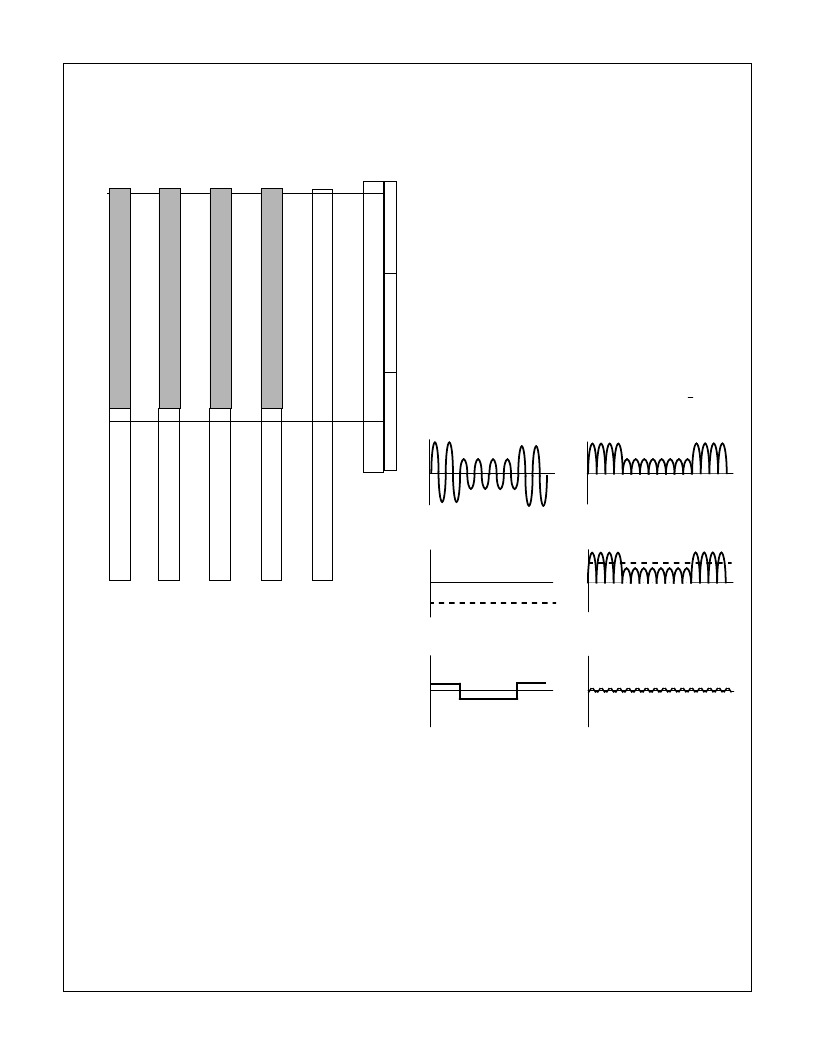
Figure 10 illustrates a typical AGC detection process.
Typically, the average input error is read from the Input Level
Detector port for use in AGC Applications. By setting the
threshold to 0, however, the average value of the input signal
can be read directly. The calculation is:
where “l(fā)evel” is the 24-bit value read from the 3 level Detec-
tor Registers and “N” is the number of samples to be inte-
grated. Note that to get the RMS value of a sinusoid, multiply
the average value of the rectified sinusoid by 1.111. For a full
scale input sinusoid, this yields an RMS value of approxi-
mately 3 dBFS.
NOTE: 1.111 scales the rectified sinusoid average (2/
π
) to 1/
√
2
.
In the HSP50214A, the polarity of the two LSB’s of the inte-
gration period pre-load is selectable. If Control Word 27, Bit
23 is set to a logic one, the two LSB’s of the integration
period preload are set to logic ones. This allows a power of
two to be set for the integration period, for easy normaliza-
tion in the processor. If Control Word 27, Bit 23 is set to a
logic zero, then the two LSB’s of the integration period pre-
load are set to zeros as in the HSP50214.
Carrier Synthesizer/Mixer
The Carrier Synthesizer/Mixer Section of the HSP50214A is
shown in Figure 12. The NCO has a 32-bit phase accumula-
tor, a 10-bit phase offset adder, and a sine/cosine ROM.
A
O
I
M
T
μ
P
2
0
2
-1
2
-2
2
-3
2
-4
2
-5
2
-6
2
-7
2
-8
2
-9
2
-10
2
-11
2
-12
2
-13
0
2
-1
2
-2
2
-3
2
-4
2
-5
2
-6
2
-7
2
-8
2
-9
2
-10
2
-11
2
-12
2
-13
-2
0
2
-1
2
-2
2
-3
2
-4
2
-5
2
-6
2
-7
2
-8
2
-9
2
-10
2
-11
2
-12
2
-13
2
0
2
-1
2
-2
2
-3
2
-4
2
-5
2
-6
2
-7
2
-8
2
-9
2
-10
2
-11
2
-12
2
-13
2
0
2
-1
2
-2
2
-3
2
-4
2
-5
2
-6
2
-7
2
-8
2
-9
2
-10
2
-11
2
-12
2
-13
FS
-6dB
-12dB
-18dB
-24dB
-30dB
-36dB
-42dB
-48dB
-54dB
-60dB
-66dB
-72dB
-78dB
2
14
2
13
2
12
2
11
2
10
2
9
2
8
2
7
2
6
2
5
2
4
2
3
2
2
2
1
2
17
2
16
2
15
2
18
2
0
2
-1
2
-2
2
-3
2
-4
2
14
2
13
2
12
2
11
2
10
2
9
2
8
2
7
2
6
2
5
2
4
2
3
2
2
2
1
2
17
2
16
2
15
2
18
0
0
0
0
R
P
A
FIGURE 10. INPUT THRESHOLD DETECTOR BIT WEIGHTING
dBFS
RMS
20
(
)
1.111
(
)
level
(
)
N
( )
16
(
)
(
)
[
]
log
=
(EQ. 2)
A
A) INPUT SIGNAL
C) THRESHOLD
B) RECTIFIED SIGNAL
D) ACCUMULATOR INPUTS
E) DETECTOR OUTPUT
A
A
A
A
A
F) CLOSED LOOP STEADY STATE
(CONSTANT INPUT)
FIGURE 11. SIGNAL PROCESSING WITHIN LEVEL DETECTOR
HSP50214A
相關(guān)PDF資料 |
PDF描述 |
|---|---|
| HSP50214AVI | Programmable Downconverter |
| HSP50214B | Programmable Downconverter |
| HSP50214BVC | Programmable Downconverter |
| HSP50214BVI | Programmable Downconverter |
| HT84 | ADSL Coupling Transformers |
相關(guān)代理商/技術(shù)參數(shù) |
參數(shù)描述 |
|---|---|
| HSP50214AVI | 制造商:INTERSIL 制造商全稱:Intersil Corporation 功能描述:Programmable Downconverter |
| HSP50214B | 制造商:INTERSIL 制造商全稱:Intersil Corporation 功能描述:Programmable Downconverter |
| HSP50214B_07 | 制造商:INTERSIL 制造商全稱:Intersil Corporation 功能描述:Programmable Downconverter |
| HSP50214BVC | 功能描述:上下轉(zhuǎn)換器 120L MQFP COMTEMP 14-BIT PROGRAMMABLE DOWNCONVERTER 65MSPS RoHS:否 制造商:Texas Instruments 產(chǎn)品:Down Converters 射頻:52 MHz to 78 MHz 中頻:300 MHz LO頻率: 功率增益: P1dB: 工作電源電壓:1.8 V, 3.3 V 工作電源電流:120 mA 最大功率耗散:1 W 最大工作溫度:+ 85 C 安裝風(fēng)格:SMD/SMT 封裝 / 箱體:PQFP-128 |
| HSP50214BVCZ | 功能描述:上下轉(zhuǎn)換器 120L MQFP COMTEMP 14-BIT PROG DWNCNVRT RoHS:否 制造商:Texas Instruments 產(chǎn)品:Down Converters 射頻:52 MHz to 78 MHz 中頻:300 MHz LO頻率: 功率增益: P1dB: 工作電源電壓:1.8 V, 3.3 V 工作電源電流:120 mA 最大功率耗散:1 W 最大工作溫度:+ 85 C 安裝風(fēng)格:SMD/SMT 封裝 / 箱體:PQFP-128 |
發(fā)布緊急采購,3分鐘左右您將得到回復(fù)。