- 您現(xiàn)在的位置:買賣IC網(wǎng) > PDF目錄383075 > HSP50214AVC (HARRIS SEMICONDUCTOR) Programmable Downconverter PDF資料下載
參數(shù)資料
| 型號(hào): | HSP50214AVC |
| 廠商: | HARRIS SEMICONDUCTOR |
| 元件分類: | 通信及網(wǎng)絡(luò) |
| 英文描述: | Programmable Downconverter |
| 中文描述: | SPECIALTY TELECOM CIRCUIT, PQFP120 |
| 文件頁數(shù): | 28/60頁 |
| 文件大?。?/td> | 467K |
| 代理商: | HSP50214AVC |
第1頁第2頁第3頁第4頁第5頁第6頁第7頁第8頁第9頁第10頁第11頁第12頁第13頁第14頁第15頁第16頁第17頁第18頁第19頁第20頁第21頁第22頁第23頁第24頁第25頁第26頁第27頁當(dāng)前第28頁第29頁第30頁第31頁第32頁第33頁第34頁第35頁第36頁第37頁第38頁第39頁第40頁第41頁第42頁第43頁第44頁第45頁第46頁第47頁第48頁第49頁第50頁第51頁第52頁第53頁第54頁第55頁第56頁第57頁第58頁第59頁第60頁
28
The programmable parameters for the Timing NCO include
an Enable External Timing NCO Sync (Control Word 11, Bit
5), the serial word width, Number of Offset Frequency Bits
(Control Word 11, Bits 3-4), an Enable Offset Frequency
control (Control Word 11, Bit 2), a Clear NCO Accumulator
control (Control Word 11, Bit 1), a Timing NCO Phase Accu-
mulator Load On Update control (Control Word 11, Bit 0), the
Timing NCO Center Frequency (Control Word 12), a Timing
Phase Offset (Control Word 13, Bits 0-7), a Timing Fre-
quency Strobe (Control Word 14) and a Timing Phase
Strobe (Control Word 15). Refer to the Carrier Synthesizer
Mixer Section for a detailed discussion of the serial interface
for the Timing NCO offset frequency word.
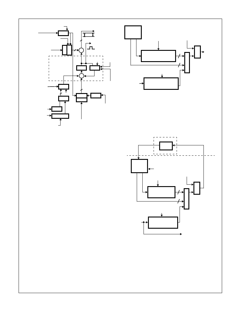
A timing error detector is provided for measuring the phase
difference between the timing NCO and a external clock input,
REFCLK. Timing Error is generated by comparing the values
of two programmable counters. One counter is clocked with
the Timing NCO carry out and the other is clocked by the
REFCLK. The 12-bit NCO Divide parameter is set in Control
Word 18, Bits 16-27. The NCO Divide parameter is the pre-
load to the counter that is clocked by the Timing NCO carry
out. The 12-bit Reference Divide parameter is set in Control
Word 18, Bits 0-11, and is the preload for the counter that is
clocked by the Reference clock. Figure 26 details the block
diagram of the timing error generation circuit. The 16 bits of
timing error are available both as a PDC serial output and as a
processor read parameter. See the Processor Read Section
for more details on accessing this value.
Figure 27A illustrates an application where the Timing Error
Generator is used to lock the receiver samples with a trans-
mit data rate. In this example, the receive samples are at
four times the transmit data rate. An external loop filter is
required, whose frequency error output is fed into the Timing
NCO. This allows the loop to track out the long term drift
between the receive sample rate and the transmit data clock.
SHIFT REG
SYNC
SOF
SOFSYNC
TIMING NCO CENTER
FREQUENCY
TIMING NCO
PHASE OFFSET
32
32
8
MUX
0
MUX
0
CLEAR
PHASE
ACC
PHASE
ACCUMULATOR
SCF
SOF
ENABLE SOF
REG
REG
+
Controlled via microprocessor interface.
5
TIMING PHASE STROBE
TIMING FREQ
STROBE
NUMBER OF SOF BITS
+
R
TIMING NCO
PH ACC
LOAD ON
UPDATE
R
REG
SYNC
SYNCIN2
EN EXT TIMING NCO SYNC
SYNC
CARRY OUT = RUN
FILTER STROBE
FILTER PHASE
SELECT
FIGURE 26. TIMING NCO BLOCK DIAGRAM
REG
Controlled via microprocessor interface.
FIGURE 27. TIMING ERROR GENERATION
PROGRAMMABLE
DIVIDER
PROGRAMMABLE
DIVIDER
REFERENCE
DIVIDE
TE(15:0)
C
REFCLK
R
+
TIMING
NCO
ACC.
P
NCO DIVIDE
(NCO DIVIDE)/2
-
12
4
EN
Controlled via microprocessor interface.
FIGURE 27A. TIMING ERROR APPLICATION
PROGRAMMABLE
DIVIDER
PROGRAMMABLE
DIVIDER
REFERENCE
DIVIDE = N
TE(15:0)
C
Tx DATA CLK
(REFCLK)
R
+
TIMING
NCO
ACC.
P
NCO DIVIDE = 4N
(NCO DIVIDE)/2
-
12
4
EN
LOOP
FILTER
μ
P
TO Tx BLOCK
(MODULATOR)
CLKIN/R
T
R
T
= TOTAL DECIMATION (CIC, HB FILTERS AND FIR)
HSP50214A
相關(guān)PDF資料 |
PDF描述 |
|---|---|
| HSP50214AVI | Programmable Downconverter |
| HSP50214B | Programmable Downconverter |
| HSP50214BVC | Programmable Downconverter |
| HSP50214BVI | Programmable Downconverter |
| HT84 | ADSL Coupling Transformers |
相關(guān)代理商/技術(shù)參數(shù) |
參數(shù)描述 |
|---|---|
| HSP50214AVI | 制造商:INTERSIL 制造商全稱:Intersil Corporation 功能描述:Programmable Downconverter |
| HSP50214B | 制造商:INTERSIL 制造商全稱:Intersil Corporation 功能描述:Programmable Downconverter |
| HSP50214B_07 | 制造商:INTERSIL 制造商全稱:Intersil Corporation 功能描述:Programmable Downconverter |
| HSP50214BVC | 功能描述:上下轉(zhuǎn)換器 120L MQFP COMTEMP 14-BIT PROGRAMMABLE DOWNCONVERTER 65MSPS RoHS:否 制造商:Texas Instruments 產(chǎn)品:Down Converters 射頻:52 MHz to 78 MHz 中頻:300 MHz LO頻率: 功率增益: P1dB: 工作電源電壓:1.8 V, 3.3 V 工作電源電流:120 mA 最大功率耗散:1 W 最大工作溫度:+ 85 C 安裝風(fēng)格:SMD/SMT 封裝 / 箱體:PQFP-128 |
| HSP50214BVCZ | 功能描述:上下轉(zhuǎn)換器 120L MQFP COMTEMP 14-BIT PROG DWNCNVRT RoHS:否 制造商:Texas Instruments 產(chǎn)品:Down Converters 射頻:52 MHz to 78 MHz 中頻:300 MHz LO頻率: 功率增益: P1dB: 工作電源電壓:1.8 V, 3.3 V 工作電源電流:120 mA 最大功率耗散:1 W 最大工作溫度:+ 85 C 安裝風(fēng)格:SMD/SMT 封裝 / 箱體:PQFP-128 |
發(fā)布緊急采購,3分鐘左右您將得到回復(fù)。