- 您現(xiàn)在的位置:買賣IC網(wǎng) > PDF目錄383075 > HSP50214AVC (HARRIS SEMICONDUCTOR) Programmable Downconverter PDF資料下載
參數(shù)資料
| 型號(hào): | HSP50214AVC |
| 廠商: | HARRIS SEMICONDUCTOR |
| 元件分類: | 通信及網(wǎng)絡(luò) |
| 英文描述: | Programmable Downconverter |
| 中文描述: | SPECIALTY TELECOM CIRCUIT, PQFP120 |
| 文件頁(yè)數(shù): | 43/60頁(yè) |
| 文件大?。?/td> | 467K |
| 代理商: | HSP50214AVC |
第1頁(yè)第2頁(yè)第3頁(yè)第4頁(yè)第5頁(yè)第6頁(yè)第7頁(yè)第8頁(yè)第9頁(yè)第10頁(yè)第11頁(yè)第12頁(yè)第13頁(yè)第14頁(yè)第15頁(yè)第16頁(yè)第17頁(yè)第18頁(yè)第19頁(yè)第20頁(yè)第21頁(yè)第22頁(yè)第23頁(yè)第24頁(yè)第25頁(yè)第26頁(yè)第27頁(yè)第28頁(yè)第29頁(yè)第30頁(yè)第31頁(yè)第32頁(yè)第33頁(yè)第34頁(yè)第35頁(yè)第36頁(yè)第37頁(yè)第38頁(yè)第39頁(yè)第40頁(yè)第41頁(yè)第42頁(yè)當(dāng)前第43頁(yè)第44頁(yè)第45頁(yè)第46頁(yè)第47頁(yè)第48頁(yè)第49頁(yè)第50頁(yè)第51頁(yè)第52頁(yè)第53頁(yè)第54頁(yè)第55頁(yè)第56頁(yè)第57頁(yè)第58頁(yè)第59頁(yè)第60頁(yè)
43
Applications
Composite Filter Response Example
For this example consider a total receive band roughly
25MHz wide containing 124 200kHz wide FDM channels as
shown in Figure 44. The design goal for the PDC is to tune to
and filter out a single 200kHz FDM channel from the FDM
band, passing only baseband samples onto the baseband
processor at a multiple of the 270.8 KBPS bit rate.
RF/IF Considerations
The input frequency to the PDC is dependent on the A/D
converter selected, the RF/IF frequency, the bandwidth of
interest and the sample rate of the converter. If the A/D con-
verter has sufficient bandwidth, then undersampling tech-
niques can be used to downconvert IF/RF frequencies as
part of the digitizing process, using the PDC to process a
lower frequency alias of the input signal.
For example, a 70MHz IF can be sampled at 40MHz and the
resulting 10MHz signal alias can be processed by the PDC
to perform the desired downconversion/tuning and filtering. If
the IF signal is less than 1/2 the sample frequency then stan-
dard oversampling techniques can be used to process the
signal. Of the two techniques, only undersampling allows
part of the down conversion function to be brought into the
digital domain just through sampling, assuming that a sam-
pling frequency can be found that keeps the alias signals low
and that the A/D converter has the bandwidth to accept the
unconverted analog signal.
TABLE 22. DEFINITION OF ADDRESS MAP
READ
CODE C2-0
STATUS
TYPE
READ ADDRESS A(2:0)
0
Buffer
RAM I and
Q
000- I LSB.
001- I MSB.
010- Q LSB.
011- Q MSB.
See Output Section.
1
Buffer
RAM
Output
(|r| and
φ)
000- MAG LSB (7-0).
001- MAG MSB (15-8).
010- PHASE LSB (7-0).
011- PHASE MSB (15-8).
See Output Section.
2
Buffered
Frequency
000- FREQ LSB.
001- FREQ MSB.
See Output Section.
3
Not Used
4
InputLevel
Detector
Input AGC
000- input AGC LSB (0-7).
001- input AGC NLSB (8-15).
010- input AGC MSB (16-23).
5
AGC Data
andTiming
Error
AGC (must write to location 10 to sample)
000- AGC LSB (lower 8 bits of linear
Control Word 3 used by multiplier)
mmmmmmmm LSB.
001- AGC MSB (4 shift control bits and
first three bits of linear) Control Word
oeeeemmm MSB. This yields 11 bits of
the linear control mantissa.
010- Timing error LSB, not stabilized.
011- Timing error MSB, not stabilized.
6
Not Used
7
Not Used
Don’t Care
Status
111- Status (6:0) consisting of
(6:4)-FIFOdepthwhenoutputisinFIFO
Buffer RAM Output Mode.
(3)-EMPTYsignallingthe FIFOisempty
and the read pointer cannot be ad-
vanced (Active High).
(2)-FULL signalling the FIFO is full and
new samples will not be written (Active
High).
(1)-READYB Output buffer has reached
the programmed threshold in FIFO
mode or the programmed number of
samples have been taken in snapshot
mode. (Active Low).
(0)-INTEGRATIONhasbeencompleted
intheinputleveldetectorandisreadyto
be read. (Active High).
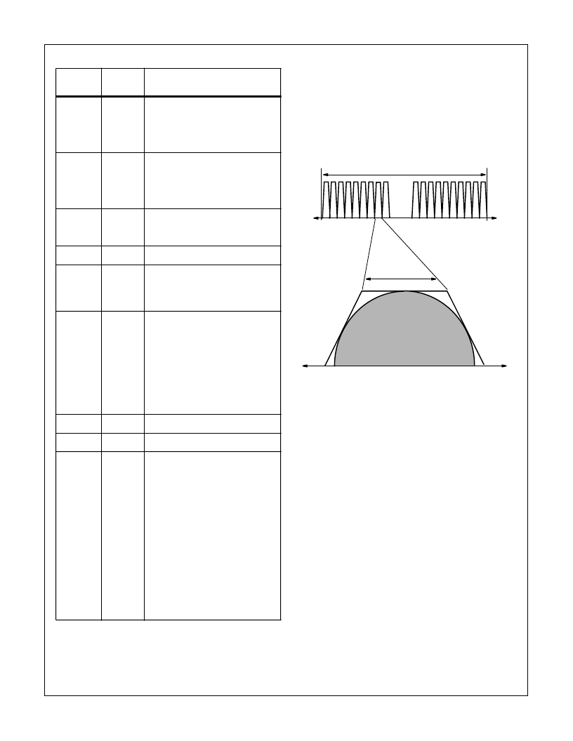
FIGURE 47. RECEIVE SIGNAL FREQUENCY SPECTRUM
FREQUENCY
FREQUENCY
124 CHANNELS
200kHz
CHANNEL
HSP50214A
相關(guān)PDF資料 |
PDF描述 |
|---|---|
| HSP50214AVI | Programmable Downconverter |
| HSP50214B | Programmable Downconverter |
| HSP50214BVC | Programmable Downconverter |
| HSP50214BVI | Programmable Downconverter |
| HT84 | ADSL Coupling Transformers |
相關(guān)代理商/技術(shù)參數(shù) |
參數(shù)描述 |
|---|---|
| HSP50214AVI | 制造商:INTERSIL 制造商全稱:Intersil Corporation 功能描述:Programmable Downconverter |
| HSP50214B | 制造商:INTERSIL 制造商全稱:Intersil Corporation 功能描述:Programmable Downconverter |
| HSP50214B_07 | 制造商:INTERSIL 制造商全稱:Intersil Corporation 功能描述:Programmable Downconverter |
| HSP50214BVC | 功能描述:上下轉(zhuǎn)換器 120L MQFP COMTEMP 14-BIT PROGRAMMABLE DOWNCONVERTER 65MSPS RoHS:否 制造商:Texas Instruments 產(chǎn)品:Down Converters 射頻:52 MHz to 78 MHz 中頻:300 MHz LO頻率: 功率增益: P1dB: 工作電源電壓:1.8 V, 3.3 V 工作電源電流:120 mA 最大功率耗散:1 W 最大工作溫度:+ 85 C 安裝風(fēng)格:SMD/SMT 封裝 / 箱體:PQFP-128 |
| HSP50214BVCZ | 功能描述:上下轉(zhuǎn)換器 120L MQFP COMTEMP 14-BIT PROG DWNCNVRT RoHS:否 制造商:Texas Instruments 產(chǎn)品:Down Converters 射頻:52 MHz to 78 MHz 中頻:300 MHz LO頻率: 功率增益: P1dB: 工作電源電壓:1.8 V, 3.3 V 工作電源電流:120 mA 最大功率耗散:1 W 最大工作溫度:+ 85 C 安裝風(fēng)格:SMD/SMT 封裝 / 箱體:PQFP-128 |
發(fā)布緊急采購(gòu),3分鐘左右您將得到回復(fù)。