- 您現(xiàn)在的位置:買賣IC網(wǎng) > PDF目錄371898 > HSP50016JC-75 (INTERSIL CORP) Digital Down Converter PDF資料下載
參數(shù)資料
| 型號: | HSP50016JC-75 |
| 廠商: | INTERSIL CORP |
| 元件分類: | 數(shù)字信號處理外設(shè) |
| 英文描述: | Digital Down Converter |
| 中文描述: | 16-BIT, DSP-MIXER, PQCC44 |
| 封裝: | PLASTIC, LCC-44 |
| 文件頁數(shù): | 13/31頁 |
| 文件大小: | 209K |
| 代理商: | HSP50016JC-75 |
第1頁第2頁第3頁第4頁第5頁第6頁第7頁第8頁第9頁第10頁第11頁第12頁當(dāng)前第13頁第14頁第15頁第16頁第17頁第18頁第19頁第20頁第21頁第22頁第23頁第24頁第25頁第26頁第27頁第28頁第29頁第30頁第31頁

3-210
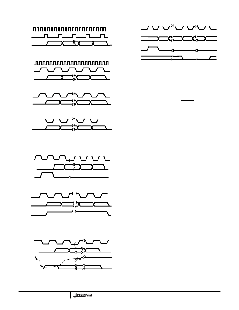
Data can be read out of the DDC on request through the use
of the IQSTRT pin. After passing through the Output
Formatter, the I and Q data are stored in output buffers,
which are updated at the end of the FIR Filter processing
cycle. The IQSTRT and IQSTB lines form a two line
handshake as shown in Figure 13. IQSTRT initiates the
request. If the buffer has data in it, the DDC will begin an
output data sequence on the next edge of IQCLK. The DDC
will then put out one bit per IQCLK until the output cycle is
complete. In I followed by Q Mode, one IQSTRT will initiate
an I output word followed by a Q output word. In real data
Output Mode, one IQSTRT will initiate two samples of real
data on the I pin.
To avoid the generation of multiple read cycles, IQSTRT
must go inactive within 10 cycles of IQCLK after the initiation
of IQSTB. The DDC will not update the output buffer again
until the current output cycle has completed. When IQSTRT
is used in this handshake mode, it must consist of pulses
that satisfy the set up and hold requirements listed in the AC
Timing Specifications and the pulses must occur at a rate of
at least CLK/(HDF Decimation Factor x 4 -1). This mode of
operation requires the Time Slot Number in Control Word 6
to be 0.
NOTE: When handshake mode is not used, IQSTRT should
be at a logic low.
Auto Three-State Mode for IQCLK, IQSTB, I and Q allows
multiple chips to operate using common data and output
control lines. Each chip is assigned a Time Slot Number on
the bus to use for outputting its data. All outputs
programmed for Auto Three-State Mode are active during
their time slot and are in a high impedance state at all other
times. A time slot starts one CLK period prior to the
beginning of the first bit of I or Q and ends (Time Slot
Length) CLK periods afterwards. Assignment of a time slot is
with reference to the deassertion of RESET. The minimum
possible Time Slot Length for a given application is:
where Mode = 2 if the DDC is in either Real Output or I
followed By Q Mode; else Mode = 1.
FIGURE 12. IQSTB TIMING
FIGURE 13. REQUESTED DATA OUTPUT TIMING
IQCLK
CLK
IQCLK
I OR Q
BIT 0
BIT 1
IQCLK
CLK
A. IQCLK DUTY CYCLE: ACTIVE TIME = CLK PERIOD
(IQCLK POLARITY = 0)
B. IQCLK DUTY CYCLE: 50%
C. IQCLK DURATION: CONTINUOUS
I OR Q
BIT 0
BIT 1
BIT N-1
BIT N
I OR Q
BIT 0
BIT 1
BIT N-1
BIT N
IQCLK
I OR Q
BIT 0
BIT 1
BIT N-1
BIT N
D. IQCLK DURATION: ACTIVE DURING I OR Q ONLY
BIT N-1
BIT N
FIGURE 11. TIMING FOR CLK, IQCLK, IQSTB, I AND Q
I/QSTB
IQCLK
I OR Q
BIT 0
BIT 1
BIT N-1
BIT N
BIT 0
BIT 1
BIT N-1
BIT N
IQSTB
IQCLK
I OR Q
A. IQSTB ACTIVE PRIOR TO DATA WORD
B. IQSTB ACTIVE DURING DATA WORD
IQSTRT
IQCLK
BIT 0
BIT N
IQSTB
I or Q
TRAILING
0
LEADING
0
FIGURE 14. CONTROL WORD TIMING DIAGRAM
BIT39
BIT0
CCLK
CSTB
CDATA
CS
BIT36
BIT35
Length
MIN
Numberof Output Bits
2
+
(
)
Mode
×
[
]
1; or
+
=
(EQ. 15)
HSP50016
相關(guān)PDF資料 |
PDF描述 |
|---|---|
| HSP50110JC-60 | Communications Tuner Circuit |
| HSP50306SC-25 | Digital QPSK Demodulator |
| HSP50306SC-2596 | Digital QPSK Demodulator |
| HSP50306SC-27 | Digital QPSK Demodulator |
| HSP50306SC-2796 | Digital QPSK Demodulator |
相關(guān)代理商/技術(shù)參數(shù) |
參數(shù)描述 |
|---|---|
| HSP50016JI-52 | 制造商:Rochester Electronics LLC 功能描述:DIGITAL DOWN CONVERTER 44 PLCC, 52MHZ, COMM,INDS - Bulk |
| HSP50016JM-5296R3571 | 制造商:Intersil Corporation 功能描述:ROCKWELL HSP50016JC-5296 W/BRAND,-55/+125C OP TEMP,ELECTR - Tape and Reel |
| HSP50016JM-52R3571 | 制造商:Rochester Electronics LLC 功能描述:- Bulk |
| HSP50110 | 制造商:INTERSIL 制造商全稱:Intersil Corporation 功能描述:Digital Quadrature Tuner |
| HSP50110_01 | 制造商:INTERSIL 制造商全稱:Intersil Corporation 功能描述:Digital Quadrature Tuner |
發(fā)布緊急采購,3分鐘左右您將得到回復(fù)。