- 您現(xiàn)在的位置:買賣IC網(wǎng) > PDF目錄371898 > HSP50016JC-75 (INTERSIL CORP) Digital Down Converter PDF資料下載
參數(shù)資料
| 型號(hào): | HSP50016JC-75 |
| 廠商: | INTERSIL CORP |
| 元件分類: | 數(shù)字信號(hào)處理外設(shè) |
| 英文描述: | Digital Down Converter |
| 中文描述: | 16-BIT, DSP-MIXER, PQCC44 |
| 封裝: | PLASTIC, LCC-44 |
| 文件頁(yè)數(shù): | 12/31頁(yè) |
| 文件大?。?/td> | 209K |
| 代理商: | HSP50016JC-75 |
第1頁(yè)第2頁(yè)第3頁(yè)第4頁(yè)第5頁(yè)第6頁(yè)第7頁(yè)第8頁(yè)第9頁(yè)第10頁(yè)第11頁(yè)當(dāng)前第12頁(yè)第13頁(yè)第14頁(yè)第15頁(yè)第16頁(yè)第17頁(yè)第18頁(yè)第19頁(yè)第20頁(yè)第21頁(yè)第22頁(yè)第23頁(yè)第24頁(yè)第25頁(yè)第26頁(yè)第27頁(yè)第28頁(yè)第29頁(yè)第30頁(yè)第31頁(yè)

3-209
Generator Carry Out will appear on the output. Control Word
5 contains fields to set the number of output bits transmitted
to the arithmetic representation and interface control of the
serial output data. Control Word 4, Bits 31-32, allow
selection of baseband centered quadrature on baseband
offset quadrature complex outputs. Control Word 4, Bit 0,
allows selection of spectral inversion. In addition, the output
drivers for I, Q, IQCLK and IQSTB can be individually
enabled or placed in a high impedance state using Control
Word 6, Bits 20-28. These options are explained below.
When the “Output Spectrum” signal (CW4, bits 31-32) is set
to “01”, then the real output data appears on the I output and
the Q output in the I/Q separate mode. When in I Mode
followed by Q Mode, the Q slot is also real data since the
real mode outputs at twice the rate of the complex mode
(CW4, bits 31-32 = 00).
When set for fixed point output, the output data can be in
two's complement, offset binary or signed magnitude form.
Data is converted to offset binary by complementing the most
significant bit of a two's complement number. The length of
the output data word can be 16, 24, 32 or 38-bits. The first
three options are symmetrically rounded to the LSB of the
output data; the fourth option represents the full 38-bit
width of the accumulator and so represents exact
arithmetic.
The output has a saturation option to prevent possible
overflow due to a step input at power up. When Overflow
Protection is enabled, the output is forced to be either the
most positive or most negative number. Saturation is
available in all four fixed point output options, and is set via
Control Word 7, Bit 0.
Data can also be output in single precision floating point
format (see Table 2). For all output data formats, the
internal calculations are performed in exact two’s
complement integer arithmetic and the resulting data is
converted in the Output Formatter.
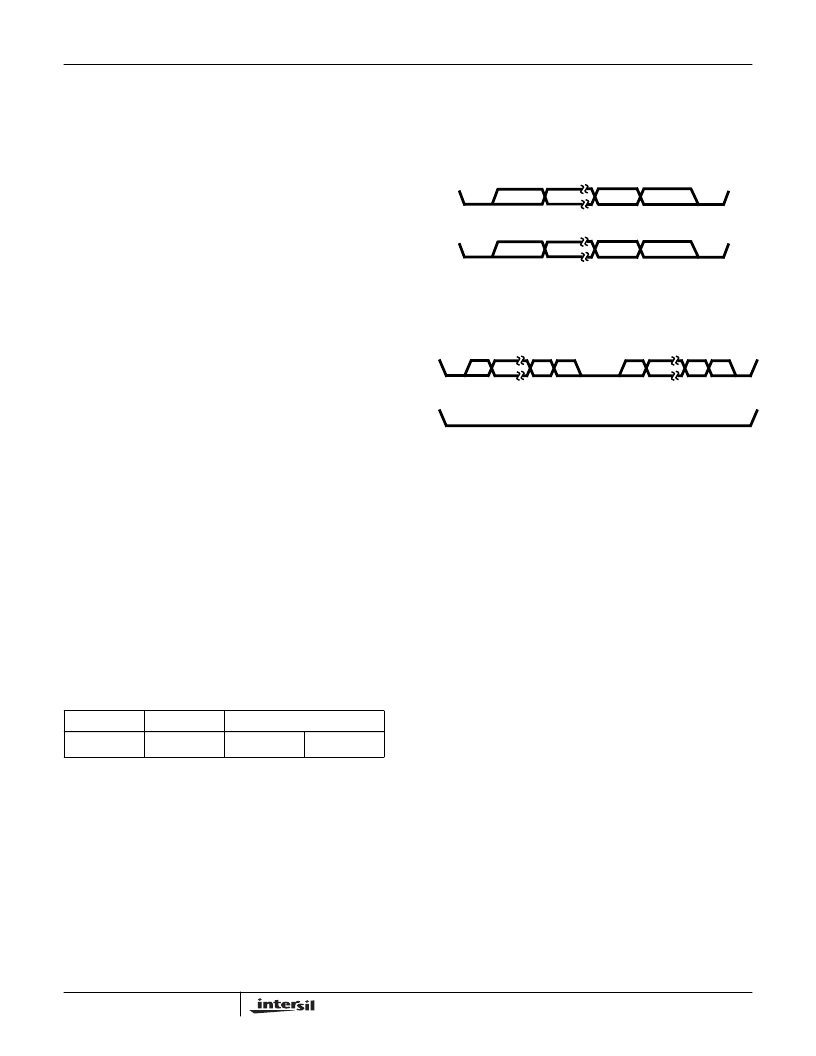
The I and Q pins can be programmed for either
simultaneous or I followed by Q output. In simultaneous
mode, the I and Q data appear on the I and Q pins,
respectively. Each data sample is preceded by a leading
zero bit, followed by the output data, followed by a trailing
zero bit. In I followed by Q Mode, the output data appears
on the I pin, and consists of a leading zero bit, then the I
data, a trailing zero, a leading zero, the Q data, and finally
a trailing zero bit. In Figures 10 through 12, the leading
and trailing zero bits occur before bit 0 and after bit N,
respectively.
IQCLK is used to delineate the bit or word timing of the I and
Q outputs. There are several options on the configuration of
IQCLK, which are controlled with Control Word 6 (see
Table 8). The frequency of IQCLK is programmed to be a
fraction of the CLK frequency, from (CLK rate)/2 to (CLK
rate)/8192 (see Equation 14). If IQCLK Rate = 0, then
IQCLK remains in its inactive state and the output bits
change on the rising edges of CLK.
IQCLK can be programmed to be active continuously, or only
during I or Q data output via the IQCLK duration bit. Using the
IQCLK Duty Cycle bit, IQCLK is selectable as either 50% duty
cycle or to be high for one period of CLK. In addition, the
Formatter can be set so that the data bits are clocked on
either the positive or negative edges of IQCLK with the IQCLK
Polarity bit. Figure 11 shows the various modes of operation
with IQCLK Polarity programmed for active high operation.
Control Word 6 also configures IQSTB, as shown in
Figure 12. When programmed for Active Prior to Data Word,
IQSTB is high for one period of IQCLK and terminates
simultaneously with the beginning of the first data bit;
otherwise it goes active with the beginning of the first bit and
inactive with the end of the last bit. IQSTB can be
programmed to be either active high or low.
TABLE 2. FLOATING POINT FORMAT
SIGN
EXPONENT
MANTISSA
-2
0
2
7
to 2
0
Implied 1
0.2
-1
to 2
-23
A. SIMULTANEOUS OUTPUT MODE
B. I FOLLOWED BY Q OUTPUT MODE
FIGURE 10. DATA OUTPUT MODES
IQCLK Rate
-------------------------------------------------
1
–
=
(EQ. 14)
N
N-1
1
0
STOP
BIT
START
BIT
N
N-1
1
0
STOP
BIT
START
BIT
I
Q
N = 16, 24, 32 OR 38
Q
Q
N
Q
N-1
STOP
BIT
STOP
BIT
I
Q
1
Q
0
START
BIT
Q
N
Q
N-1
Q
1
Q
0
START
BIT
HSP50016
相關(guān)PDF資料 |
PDF描述 |
|---|---|
| HSP50110JC-60 | Communications Tuner Circuit |
| HSP50306SC-25 | Digital QPSK Demodulator |
| HSP50306SC-2596 | Digital QPSK Demodulator |
| HSP50306SC-27 | Digital QPSK Demodulator |
| HSP50306SC-2796 | Digital QPSK Demodulator |
相關(guān)代理商/技術(shù)參數(shù) |
參數(shù)描述 |
|---|---|
| HSP50016JI-52 | 制造商:Rochester Electronics LLC 功能描述:DIGITAL DOWN CONVERTER 44 PLCC, 52MHZ, COMM,INDS - Bulk |
| HSP50016JM-5296R3571 | 制造商:Intersil Corporation 功能描述:ROCKWELL HSP50016JC-5296 W/BRAND,-55/+125C OP TEMP,ELECTR - Tape and Reel |
| HSP50016JM-52R3571 | 制造商:Rochester Electronics LLC 功能描述:- Bulk |
| HSP50110 | 制造商:INTERSIL 制造商全稱:Intersil Corporation 功能描述:Digital Quadrature Tuner |
| HSP50110_01 | 制造商:INTERSIL 制造商全稱:Intersil Corporation 功能描述:Digital Quadrature Tuner |
發(fā)布緊急采購(gòu),3分鐘左右您將得到回復(fù)。