- 您現(xiàn)在的位置:買賣IC網(wǎng) > PDF目錄370213 > FMS988AKAC140 Signal Conditioner PDF資料下載
參數(shù)資料
| 型號: | FMS988AKAC140 |
| 英文描述: | Signal Conditioner |
| 中文描述: | 信號調(diào)理 |
| 文件頁數(shù): | 16/29頁 |
| 文件大小: | 481K |
| 代理商: | FMS988AKAC140 |
第1頁第2頁第3頁第4頁第5頁第6頁第7頁第8頁第9頁第10頁第11頁第12頁第13頁第14頁第15頁當(dāng)前第16頁第17頁第18頁第19頁第20頁第21頁第22頁第23頁第24頁第25頁第26頁第27頁第28頁第29頁

PRODUCT SPECIFICATION
FMS9875
16
REV. 1.2.15 1/14/02
Timing and Control
Timing and Control logic encompasses the PLL, Timing
Generator and Sync Stripper.
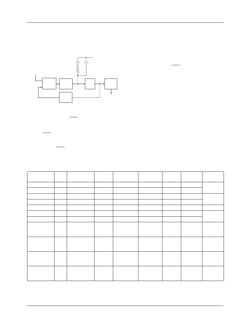
Phase Locked Loop
Two clock types originate in the PLL:
1.
Data clocks DCK and DCK.
2.
Internal sampling clock SCK.
DCK and DCK are used to strobe data from the FMS9875 to
following digital circuits. SCK is the ADC sample clock
which has adjustable phase controlled through the PHASE
register. DCK and DCK are phase aligned with SCK.
Reference for the PLL is the horizontal sync input, HSIN
with polarity selected by the HSPOL bit.
Frequency of the HS
IN
input is multiplied by the value PLLN
+ 1 derived from the PLLN
11-4
and PLLN
3-0
registers. PLLN
+ 1 should equal the number of pixels per horizontal line
including active and blanked sections. Typically blanking is
20–30% of active pixels. Divide ratios from 2–4095 are
supported. SCK, DCK and DCK run at a rate PLLN + 1
times the HS
IN
frequency.
The PLL consists of a phase comparator, charge pump VCO
and
÷
N counter, with the charge pump connected through the
LPF pin to an external filter. These elements must be pro-
grammed to match the incoming video source to be captured.
Values of IPUMP and FVCO for common video standards
timing are shown in Table 7. Timing of many computer video
outputs does not comply with VESA recommendations.
PLLN should be optimized to avoid vertical noise bars on the
displayed image.
Modes marked 2X are 2X-oversampled modes where the
number of samples per horizontal line is doubled. To select
this mode, the Phase-locked Loop Divide Ratio value must
changed from PLL
1x
to:
PLL
2x
2
=
HSIN
/N
i
o
Phase
Detector
Charge
Pump
VCO
K
V
Sub-
divider
SCK
(DCK)
I
P
C1
C2
V
Z
V
DDP
Divider
Θ
Θ
o
Θ
R
PLL
1x
1
+
(
)
1
–
Notes:
1. VESA Monitor Timing Standards and Guidelines, September 17, 1998 and others.
2. Frame refresh rate is twice the field refresh rate for interlace (i) formats and equal to the field rate for progressive (p) formats.
3. When SUBDIV
1-0
= 2, VCO runs at 2x sample rate.
Table 7. Recommended IPUMP and FVCO values for Standard Display Formats
Standard
NTSC-601
PAL-601
NTSC-601
PAL-601
SMPTE 293M
SMPTE 296M
SMPTE 274M
VGA
Test
Rank
C
C
C
C
C
C
C
C
C
C
C
C
CT
C
C
C
C
CT
CT
Resolution
720 x 483i (1X)
720 x 583i (1X)
720 x 483i (2X)
720 x 583i (2X)
720 x 483p
1280 x 720p
1920 x 1080i
640 X 480
Refresh
Rate
30 Hz
25 Hz
30 Hz
25 Hz
60 Hz
60 Hz
30 Hz
60 Hz
75 Hz
85 Hz
60 Hz
75 Hz
85 Hz
60 Hz
75 Hz
85 Hz
60 Hz
72 Hz
75 Hz
Horizontal
Frequency
15.734 kHz
15.625 kHz
15.734 kHz
15.625 kHz
31.4685 kHz
45.00 kHz
33.750 kHz
31.5 kHz
37.5 kHz
43.3 kHz
37.9 kHz
46.9 kHz
53.7 kHz
48.4 kHz
60.0 kHz
68.3 kHz
64.0 kHz
78.1 kHz
80.0 kHz
Sample Rate FVCO
1-0
13.5 MHz
13.5 MHz
27 MHz
27 MHz
27 MHz
74.25 MHz
74.25 MHz
25.175 MHz
31.500 MHz
36.000 MHz
40.000 MHz
49.500 MHz
56.250 MHz
65.000 MHz
78.750 MHz
94.500 MHz
108.000 MHz
135.000 MHz
135.000 MHz
IPUMP
2-0
101
101
101
101
111
111
111
110
110
110
110
110
110
110
110
110
110
111
111
SUBDIV
1-0
00
00
00
00
00
01
01
01
01
01
01
01
01
10
10
11
11
11
11
2
1
2
1
2
SVGA
800 X 600
1
XGA
1024 X 768
1
SXGA
1280 X 1024
1
相關(guān)PDF資料 |
PDF描述 |
|---|---|
| FMU1 | TRANSISTOR | SOT-143R |
| RU101K | TRANSISTOR | SOT-23 |
| FMU3-48R000 | Logic IC |
| FMU3-48R000M | Logic IC |
| FMU3-60R000 | Logic IC |
相關(guān)代理商/技術(shù)參數(shù) |
參數(shù)描述 |
|---|---|
| FMSA125 | 制造商:MicroSwitch 功能描述:4-DAY SHIPPING -Inductive |
| FMSA-461 | 制造商:INTERPOINT 制造商全稱:INTERPOINT 功能描述:EMI INPUT FILTER 28 VOLT INPUT |
| FMSA-461/883 | 制造商:INTERPOINT 制造商全稱:INTERPOINT 功能描述:EMI INPUT FILTER 28 VOLT INPUT |
| FMS-A-C0 | 制造商:Panduit Corp 功能描述: |
| FMSC1125-W | 制造商:FLORIDA MISC. 功能描述: |
發(fā)布緊急采購,3分鐘左右您將得到回復(fù)。