- 您現(xiàn)在的位置:買賣IC網(wǎng) > PDF目錄366550 > AM79C973 (Advanced Micro Devices, Inc.) PCnet⑩-FAST III Single-Chip 10/100 Mbps PCI Ethernet Controller with Integrated PHY PDF資料下載
參數(shù)資料
| 型號(hào): | AM79C973 |
| 廠商: | Advanced Micro Devices, Inc. |
| 英文描述: | PCnet⑩-FAST III Single-Chip 10/100 Mbps PCI Ethernet Controller with Integrated PHY |
| 中文描述: | PCnet⑩快速三單芯片10/100 Mbps的PCI以太網(wǎng)控制器集成PHY |
| 文件頁(yè)數(shù): | 106/304頁(yè) |
| 文件大小: | 2092K |
| 代理商: | AM79C973 |
第1頁(yè)第2頁(yè)第3頁(yè)第4頁(yè)第5頁(yè)第6頁(yè)第7頁(yè)第8頁(yè)第9頁(yè)第10頁(yè)第11頁(yè)第12頁(yè)第13頁(yè)第14頁(yè)第15頁(yè)第16頁(yè)第17頁(yè)第18頁(yè)第19頁(yè)第20頁(yè)第21頁(yè)第22頁(yè)第23頁(yè)第24頁(yè)第25頁(yè)第26頁(yè)第27頁(yè)第28頁(yè)第29頁(yè)第30頁(yè)第31頁(yè)第32頁(yè)第33頁(yè)第34頁(yè)第35頁(yè)第36頁(yè)第37頁(yè)第38頁(yè)第39頁(yè)第40頁(yè)第41頁(yè)第42頁(yè)第43頁(yè)第44頁(yè)第45頁(yè)第46頁(yè)第47頁(yè)第48頁(yè)第49頁(yè)第50頁(yè)第51頁(yè)第52頁(yè)第53頁(yè)第54頁(yè)第55頁(yè)第56頁(yè)第57頁(yè)第58頁(yè)第59頁(yè)第60頁(yè)第61頁(yè)第62頁(yè)第63頁(yè)第64頁(yè)第65頁(yè)第66頁(yè)第67頁(yè)第68頁(yè)第69頁(yè)第70頁(yè)第71頁(yè)第72頁(yè)第73頁(yè)第74頁(yè)第75頁(yè)第76頁(yè)第77頁(yè)第78頁(yè)第79頁(yè)第80頁(yè)第81頁(yè)第82頁(yè)第83頁(yè)第84頁(yè)第85頁(yè)第86頁(yè)第87頁(yè)第88頁(yè)第89頁(yè)第90頁(yè)第91頁(yè)第92頁(yè)第93頁(yè)第94頁(yè)第95頁(yè)第96頁(yè)第97頁(yè)第98頁(yè)第99頁(yè)第100頁(yè)第101頁(yè)第102頁(yè)第103頁(yè)第104頁(yè)第105頁(yè)當(dāng)前第106頁(yè)第107頁(yè)第108頁(yè)第109頁(yè)第110頁(yè)第111頁(yè)第112頁(yè)第113頁(yè)第114頁(yè)第115頁(yè)第116頁(yè)第117頁(yè)第118頁(yè)第119頁(yè)第120頁(yè)第121頁(yè)第122頁(yè)第123頁(yè)第124頁(yè)第125頁(yè)第126頁(yè)第127頁(yè)第128頁(yè)第129頁(yè)第130頁(yè)第131頁(yè)第132頁(yè)第133頁(yè)第134頁(yè)第135頁(yè)第136頁(yè)第137頁(yè)第138頁(yè)第139頁(yè)第140頁(yè)第141頁(yè)第142頁(yè)第143頁(yè)第144頁(yè)第145頁(yè)第146頁(yè)第147頁(yè)第148頁(yè)第149頁(yè)第150頁(yè)第151頁(yè)第152頁(yè)第153頁(yè)第154頁(yè)第155頁(yè)第156頁(yè)第157頁(yè)第158頁(yè)第159頁(yè)第160頁(yè)第161頁(yè)第162頁(yè)第163頁(yè)第164頁(yè)第165頁(yè)第166頁(yè)第167頁(yè)第168頁(yè)第169頁(yè)第170頁(yè)第171頁(yè)第172頁(yè)第173頁(yè)第174頁(yè)第175頁(yè)第176頁(yè)第177頁(yè)第178頁(yè)第179頁(yè)第180頁(yè)第181頁(yè)第182頁(yè)第183頁(yè)第184頁(yè)第185頁(yè)第186頁(yè)第187頁(yè)第188頁(yè)第189頁(yè)第190頁(yè)第191頁(yè)第192頁(yè)第193頁(yè)第194頁(yè)第195頁(yè)第196頁(yè)第197頁(yè)第198頁(yè)第199頁(yè)第200頁(yè)第201頁(yè)第202頁(yè)第203頁(yè)第204頁(yè)第205頁(yè)第206頁(yè)第207頁(yè)第208頁(yè)第209頁(yè)第210頁(yè)第211頁(yè)第212頁(yè)第213頁(yè)第214頁(yè)第215頁(yè)第216頁(yè)第217頁(yè)第218頁(yè)第219頁(yè)第220頁(yè)第221頁(yè)第222頁(yè)第223頁(yè)第224頁(yè)第225頁(yè)第226頁(yè)第227頁(yè)第228頁(yè)第229頁(yè)第230頁(yè)第231頁(yè)第232頁(yè)第233頁(yè)第234頁(yè)第235頁(yè)第236頁(yè)第237頁(yè)第238頁(yè)第239頁(yè)第240頁(yè)第241頁(yè)第242頁(yè)第243頁(yè)第244頁(yè)第245頁(yè)第246頁(yè)第247頁(yè)第248頁(yè)第249頁(yè)第250頁(yè)第251頁(yè)第252頁(yè)第253頁(yè)第254頁(yè)第255頁(yè)第256頁(yè)第257頁(yè)第258頁(yè)第259頁(yè)第260頁(yè)第261頁(yè)第262頁(yè)第263頁(yè)第264頁(yè)第265頁(yè)第266頁(yè)第267頁(yè)第268頁(yè)第269頁(yè)第270頁(yè)第271頁(yè)第272頁(yè)第273頁(yè)第274頁(yè)第275頁(yè)第276頁(yè)第277頁(yè)第278頁(yè)第279頁(yè)第280頁(yè)第281頁(yè)第282頁(yè)第283頁(yè)第284頁(yè)第285頁(yè)第286頁(yè)第287頁(yè)第288頁(yè)第289頁(yè)第290頁(yè)第291頁(yè)第292頁(yè)第293頁(yè)第294頁(yè)第295頁(yè)第296頁(yè)第297頁(yè)第298頁(yè)第299頁(yè)第300頁(yè)第301頁(yè)第302頁(yè)第303頁(yè)第304頁(yè)
106
Am79C973/Am79C975
P R E L I M I N A R Y
When the Am79C973/Am79C975 controller detects a
Magic Packet frame, it sets the MPMAT bit (CSR116,
bit 5), the MPINT bit (CSR5, bit 4), and the
PME_STATUS bit (PMCSR, bit 15). The setting of the
MPMAT bit will also cause the RWU pin to be asserted
and if the PME_EN or the PME_EN_OVR bits are set,
then the PME will be asserted as well. If IENA (CSR0,
bit 6) and MPINTE (CSR5, bit 3) are set to 1, INTA will
be asserted. Any one of the four LED pins can be pro-
grammed to indicate that a Magic Packet frame has
been received. MPSE (BCR4-7, bit 9) must be set to 1
to enable that function.
Note:
The polarity of the LED pin can be programmed
to be active HIGH by setting LEDPOL (BCR4-7, bit 14)
to 1.
Once a Magic Packet frame is detected, the
Am79C973/Am79C975 controller will discard the frame
internally, but will not resume normal transmit and re-
ceive operations until PG is asserted or MPEN is
cleared. Once both of these events has occurred, indi-
cating that the system has detected the Magic Packet
and is awake, the controller will continue polling receive
and transmit descriptor rings where it left off. It is not
necessary to re-initialize the device. If the part is re-ini-
tialized, then the descriptor locations will be reset and
the Am79C973/Am79C975 controller will not start
where it left off.
If magic packet mode is disabled by the assertion of
PG, then in order to immediately re-enable Magic
Packet mode, the PG pin must remain deasserted for
at least 200 ns before it is reasserted. If Magic Packet
mode is disabled by clearing MPEN bit, then it may be
immediately re-enabled by setting MPEN back to 1.
The PCI bus interface clock (CLK) is not required to be
running while the device is operating in Magic Packet
mode. Either of the INTA, the LED pins, RWU or the
PME signal may be used to indicate the receipt of a
Magic Packet frame when the CLK is stopped. If the
system wishes to stop the CLK, it will do so after en-
abling the Magic Packet mode.
CAUTION:
To prevent unwanted interrupts from other
active parts of the Am79C973/Am79C975 controller,
care must be taken to mask all likely interruptible
events during Magic Packet mode. An example would
be the interrupts from the Media Independent Interface,
which could occur while the device is in Magic Packet
mode.
IEEE 1149.1 (1990) Test Access Port
Interface
An IEEE 1149.1-compatible boundary scan Test Ac-
cess Port is provided for board-level continuity test and
diagnostics. All digital input, output, and input/output
pins are tested. The following paragraphs summarize
the IEEE 1149.1-compatible test functions imple-
mented in the Am79C973/Am79C975 controller.
Boundary Scan Circuit
The boundary scan test circuit requires four pins (TCK,
TMS, TDI, and TDO), defined as the Test Access Port
(TAP). It includes a finite state machine (FSM), an in-
struction register, a data register array, and a power-on
reset circuit. Internal pull-up resistors are provided for
the TDI, TCK, and TMS pins.
TAP Finite State Machine
The TAP engine is a 16-state finite state machine
(FSM), driven by the Test Clock (TCK), and the Test
Mode Select (TMS) pins. An independent power-on
reset circuit is provided to ensure that the FSM is in the
TEST_LOGIC_RESET state at power-up. Therefore,
the TRST is not provided. The FSM is also reset when
TMS and TDI are high for five TCK periods.
Supported Instructions
In addition to the minimum IEEE 1149.1 requirements
(BYPASS, EXTEST, and SAMPLE instructions), three
additional instructions (IDCODE, TRIBYP, and SET-
BYP) are provided to further ease board-level testing.
All unused instruction codes are reserved. See Table
16 for a summary of supported instructions.
Instruction Register and Decoding Logic
After the TAP FSM is reset, the IDCODE instruction is
always invoked. The decoding logic gives signals to con-
trol the data flow in the Data registers according to the
current instruction.
Boundary Scan Register
Each Boundary Scan Register (BSR) cell has two
stages. A flip-flop and a latch are used for the Serial
Shift Stage and the Parallel Output Stage, respectively.
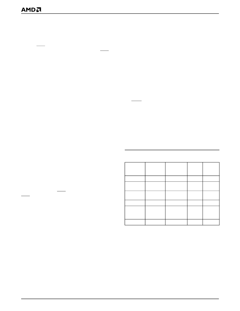
Table 16. IEEE 1149.1 Supported Instruction
Summary
Instruction
Name
EXTEST
Instruction
Code
0000
Description
External Test
ID Code
Inspection
Sample
Boundary
Force Float
Control
Boundary To
1/0
Bypass Scan
Mode
Test
Selected
Data
Register
BSR
IDCODE
0001
Normal
ID REG
SAMPLE
0010
Normal
BSR
TRIBYP
0011
Normal
Bypass
SETBYP
0100
Test
Bypass
BYPASS
1111
Normal
Bypass
相關(guān)PDF資料 |
PDF描述 |
|---|---|
| AM79C973KCW | PCnet⑩-FAST III Single-Chip 10/100 Mbps PCI Ethernet Controller with Integrated PHY |
| AM79C975KCW | PCnet⑩-FAST III Single-Chip 10/100 Mbps PCI Ethernet Controller with Integrated PHY |
| AM79C973VCW | PCnet⑩-FAST III Single-Chip 10/100 Mbps PCI Ethernet Controller with Integrated PHY |
| AM79C975VCW | PCnet⑩-FAST III Single-Chip 10/100 Mbps PCI Ethernet Controller with Integrated PHY |
| AM79C976 | PCnet-PRO⑩ 10/100 Mbps PCI Ethernet Controller |
相關(guān)代理商/技術(shù)參數(shù) |
參數(shù)描述 |
|---|---|
| AM79C973/75 | 制造商:未知廠家 制造商全稱:未知廠家 功能描述:Board Layout Considerations for the Am79C973/75 Network Interface? - (PDF) |
| AM79C973/AM79C975 | 制造商:AMD 制造商全稱:Advanced Micro Devices 功能描述:Am79C973/Am79C975 - PCnet-FAST III Single-Chip 10/100 Mbps PCI Ethernet Controller with Integrated PHY |
| AM79C973AVC\\W | 制造商:Advanced Micro Devices 功能描述: |
| AM79C973AVC\W | 制造商:Advanced Micro Devices 功能描述: |
| AM79C973BKC | 制造商:Advanced Micro Devices 功能描述:79C973BKC |
發(fā)布緊急采購(gòu),3分鐘左右您將得到回復(fù)。