- 您現(xiàn)在的位置:買賣IC網(wǎng) > PDF目錄67322 > 5962-0924001VXC (TEXAS INSTRUMENTS INC) 1-CH 12-BIT PROPRIETARY METHOD ADC, PARALLEL ACCESS, CQFP100 PDF資料下載
參數(shù)資料
| 型號(hào): | 5962-0924001VXC |
| 廠商: | TEXAS INSTRUMENTS INC |
| 元件分類: | ADC |
| 英文描述: | 1-CH 12-BIT PROPRIETARY METHOD ADC, PARALLEL ACCESS, CQFP100 |
| 封裝: | HERMETIC SEALED, CERAMIC, QFP-100 |
| 文件頁數(shù): | 8/46頁 |
| 文件大小: | 1109K |
| 代理商: | 5962-0924001VXC |
第1頁第2頁第3頁第4頁第5頁第6頁第7頁當(dāng)前第8頁第9頁第10頁第11頁第12頁第13頁第14頁第15頁第16頁第17頁第18頁第19頁第20頁第21頁第22頁第23頁第24頁第25頁第26頁第27頁第28頁第29頁第30頁第31頁第32頁第33頁第34頁第35頁第36頁第37頁第38頁第39頁第40頁第41頁第42頁第43頁第44頁第45頁第46頁
SLAS669B
– SEPTEMBER 2010 – REVISED MAY 2011
SERIAL INTERFACE
The serial port of the ADS5400 is a flexible serial interface which communicates with industry standard
microprocessors and microcontrollers. The interface provides read/write access to all registers used to define the
operating modes of ADS5400. It is compatible with most synchronous transfer formats and can be configured as
a 3 or 4 pin interface in register 0x01h. In both configurations, SCLK is the serial interface input clock and
SDENB is serial interface enable. For 3 pin configuration, SDIO is a bidirectional pin for both data in and data
out. For 4 pin configuration, SDIO is data in only and SDO is data out only.
Each read/write operation is framed by signal SDENB (Serial Data Enable Bar) asserted low for 2 to 5 bytes,
depending on the data length to be transferred (1
–4 bytes). The first frame byte is the instruction cycle which
identifies the following data transfer cycle as read or write, how many bytes to transfer, and what address to
transfer the data. Table 3 indicates the function of each bit in the instruction cycle and is followed by a detailed
description of each bit. Frame bytes 2 to 5 comprise the data transfer cycle.
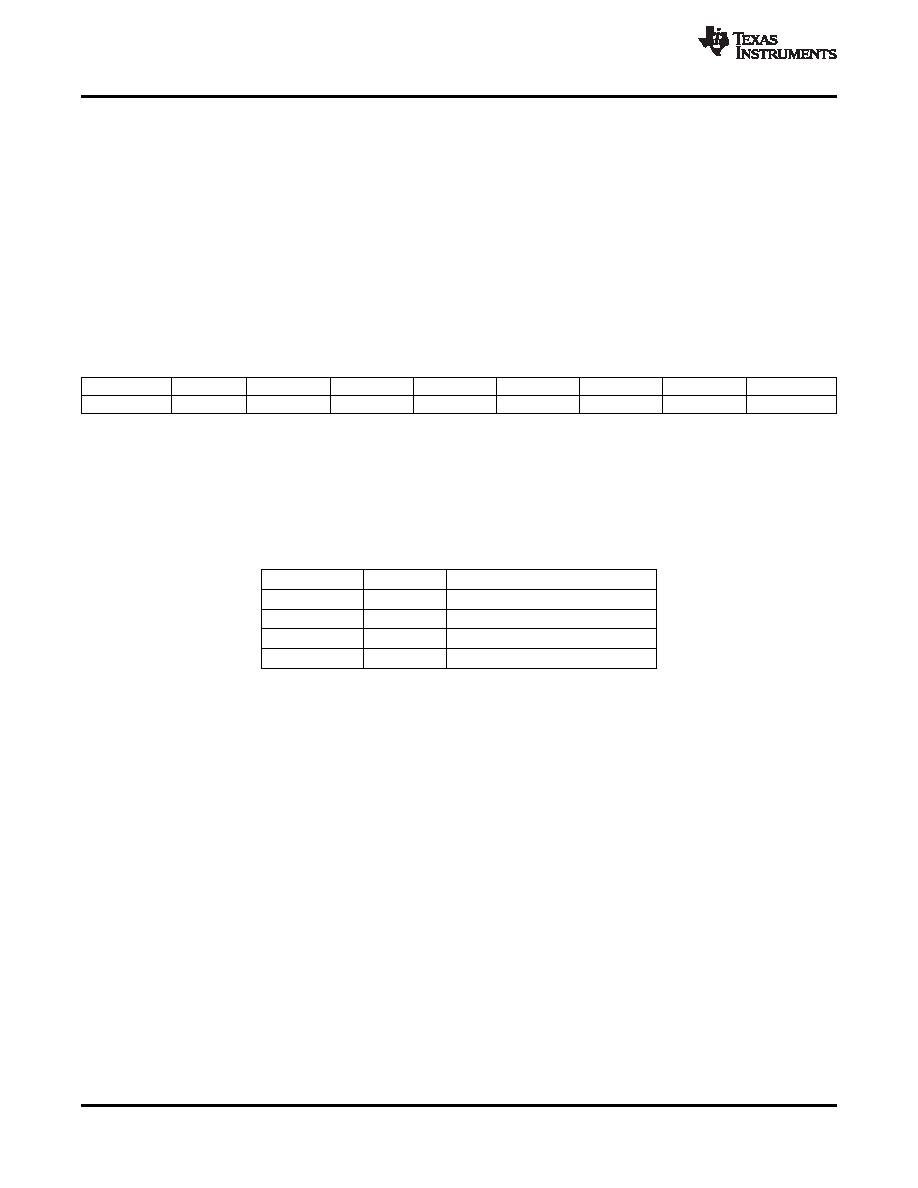
Table 3. Instruction Byte of the Serial Interface
MSB
LSB
Bit
7
6
5
4
3
2
1
0
Description
R/W
N1
N0
A4
A3
A2
A1
A0
R/W
Identifies the following data transfer cycle as a read or write operation. A high indicates a read
operation from ADS5400 and a low indicates a write operation to the ADS5400.
[N1:N0]
Identifies the number of data bytes to be transferred per Table 4 below. Data is transferred MSB
first.
Table 4. Number of Transferred Bytes Within One
Communication Frame
N1
N0
Description
0
Transfer 1 Byte
0
1
Transfer 2 Bytes
1
0
Transfer 3 Bytes
1
Transfer 4 Bytes
[A4:A0]
Identifies the address of the register to be accessed during the read or write operation. For
multi-byte transfers, this address is the starting address. Note that the address is written to the
ADS5400 MSB first and counts down for each byte.
Figure 6 shows the serial interface timing diagram for a ADS5400 write operation. SCLK is the serial interface
clock input to ADS5400. Serial data enable SDENB is an active low input to ADS5400. SDIO is serial data in.
Input data to ADS5400 is clocked on the rising edges of SCLK.
16
Copyright
2010–2011, Texas Instruments Incorporated
相關(guān)PDF資料 |
PDF描述 |
|---|---|
| 5962-3870702MGX | SWITCHED CAPACITOR CONVERTER, MBCY8 |
| 5962-3870702MPX | SWITCHED CAPACITOR CONVERTER, CDIP8 |
| 5962-8512701XC | 1-CH 12-BIT SUCCESSIVE APPROXIMATION ADC, PARALLEL ACCESS, CDIP28 |
| 5962-85127023A | 1-CH 12-BIT SUCCESSIVE APPROXIMATION ADC, PARALLEL ACCESS, CQCC28 |
| 5962-8512702XA | 1-CH 12-BIT SUCCESSIVE APPROXIMATION ADC, PARALLEL ACCESS, CDIP28 |
相關(guān)代理商/技術(shù)參數(shù) |
參數(shù)描述 |
|---|---|
| 5962-1022101VSC | 制造商:Texas Instruments 功能描述:HIGH TEMP BUCK CONVERTER - Trays |
| 5962-1123701VXC | 功能描述:靜態(tài)隨機(jī)存取存儲(chǔ)器 16MB Radiation- Hardened 靜態(tài)隨機(jī)存取存儲(chǔ)器 RoHS:否 制造商:Cypress Semiconductor 存儲(chǔ)容量:16 Mbit 組織:1 M x 16 訪問時(shí)間:55 ns 電源電壓-最大:3.6 V 電源電壓-最小:2.2 V 最大工作電流:22 uA 最大工作溫度:+ 85 C 最小工作溫度:- 40 C 安裝風(fēng)格:SMD/SMT 封裝 / 箱體:TSOP-48 封裝:Tray |
| 5962-1124201VFA | 功能描述:LVDS 接口集成電路 2x2 Crosspoint Sw RoHS:否 制造商:Texas Instruments 激勵(lì)器數(shù)量:4 接收機(jī)數(shù)量:4 數(shù)據(jù)速率:155.5 Mbps 工作電源電壓:5 V 最大功率耗散:1025 mW 最大工作溫度:+ 85 C 封裝 / 箱體:SOIC-16 Narrow 封裝:Reel |
| 596-2114-013 | 制造商:Johnson Components 功能描述:WASHER - Bulk |
| 5962-1222401QHA | 功能描述:低壓差控制器 - LDO Lo-NOISE FAST-TRANS 1.5A LDO VTG Reg RoHS:否 制造商:Micrel 最大輸入電壓:5.5 V 輸出電壓:Adjustable 輸出電流:10 mA 負(fù)載調(diào)節(jié): 輸出類型:Adjustable, Fixed 輸出端數(shù)量:1 最大工作溫度:+ 125 C 安裝風(fēng)格:SMD/SMT 封裝 / 箱體:SOT-23-6 |
發(fā)布緊急采購,3分鐘左右您將得到回復(fù)。