- 您現(xiàn)在的位置:買賣IC網(wǎng) > PDF目錄33795 > 4571 (Renesas Technology Corp.) SINGLE-CHIP 4-BIT CMOS MICROCOMPUTER PDF資料下載
參數(shù)資料
| 型號: | 4571 |
| 廠商: | Renesas Technology Corp. |
| 英文描述: | SINGLE-CHIP 4-BIT CMOS MICROCOMPUTER |
| 中文描述: | 單芯片4位微機的CMOS |
| 文件頁數(shù): | 87/126頁 |
| 文件大小: | 1627K |
| 代理商: | 4571 |
第1頁第2頁第3頁第4頁第5頁第6頁第7頁第8頁第9頁第10頁第11頁第12頁第13頁第14頁第15頁第16頁第17頁第18頁第19頁第20頁第21頁第22頁第23頁第24頁第25頁第26頁第27頁第28頁第29頁第30頁第31頁第32頁第33頁第34頁第35頁第36頁第37頁第38頁第39頁第40頁第41頁第42頁第43頁第44頁第45頁第46頁第47頁第48頁第49頁第50頁第51頁第52頁第53頁第54頁第55頁第56頁第57頁第58頁第59頁第60頁第61頁第62頁第63頁第64頁第65頁第66頁第67頁第68頁第69頁第70頁第71頁第72頁第73頁第74頁第75頁第76頁第77頁第78頁第79頁第80頁第81頁第82頁第83頁第84頁第85頁第86頁當前第87頁第88頁第89頁第90頁第91頁第92頁第93頁第94頁第95頁第96頁第97頁第98頁第99頁第100頁第101頁第102頁第103頁第104頁第105頁第106頁第107頁第108頁第109頁第110頁第111頁第112頁第113頁第114頁第115頁第116頁第117頁第118頁第119頁第120頁第121頁第122頁第123頁第124頁第125頁第126頁
Rev.1.02
May 25, 2007
Page 63 of 124
REJ03B0179-0102
4571 Group
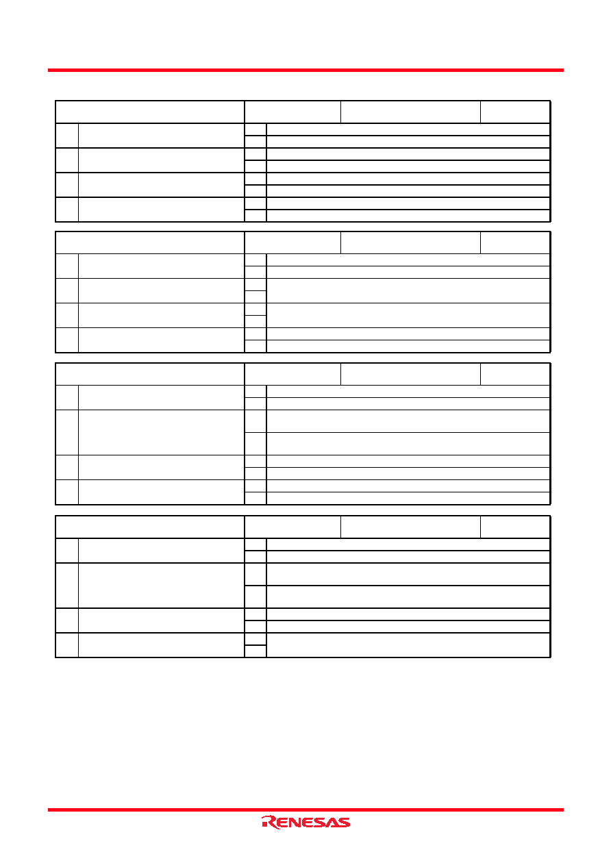
CONTROL REGISTERS
Note 1.”R” represents read enabled, and “W” represents write enabled.
Note 2.When the contents of I12 and I13 are changed, the external interrupt request flag EXF0 may be set.
Note 3.When the contents of I22 and I23 are changed, the external interrupt request flag EXF1 may be set.
Interrupt control register V1
at reset : 00002
at RAM back-up : 00002
R/W
TAV1/TV1A
V13
Timer 2 interrupt enable bit
0
Interrupt disabled (SNZT2 instruction is valid)
1
Interrupt enabled (SNZT2 instruction is invalid)
V12
Timer 1 interrupt enable bit
0
Interrupt disabled (SNZT1 instruction is valid)
1
Interrupt enabled (SNZT1 instruction is invalid)
V11
External 1 interrupt enable bit
0
Interrupt disabled (SNZ1 instruction is valid)
1
Interrupt enabled (SNZ1 instruction is invalid)
V10
External 0 interrupt enable bit
0
Interrupt disabled (SNZ0 instruction is valid)
1
Interrupt enabled (SNZ0 instruction is invalid)
Interrupt control register V2
at reset : 00002
at RAM back-up : 00002
R/W
TAV2/TV2A
V23
Voltage drop detector interrupt enable bit
0
Interrupt disabled (SNZVD instruction is valid)
1
Interrupt enabled (SNZVD instruction is invalid)
V22
Not used
0
This bit has no function, but read/write is enabled.
1
V21
Not used
0
This bit has no function, but read/write is enabled.
1
V20
Timer 3 interrupt enable bit
0
Interrupt disabled (SNZT3 instruction is valid)
1
Interrupt enabled (SNZT3 instruction is invalid)
Interrupt control register I1
at reset : 00002
at RAM back-up : state retained
R/W
TAI1/TI1A
I13
INT0 pin input control bit (Note 2)
0
INT0 pin input disabled
1
INT0 pin input enabled
I12
Interrupt valid waveform for INT0 pin/
return level selection bit (Note 2)
0
Falling waveform (“L” level of INT0 pin is recognized with the SNZI0
instruction)/“L” level
1
Rising waveform (“H” level of INT0 pin is recognized with the SNZI0
instruction)/“H” level
I11
INT0 pin edge detection circuit control bit
0
One-sided edge detected
1
Both edges detected
I10
INT0 pin
timer 1 control enable bit
0
Timer 1 disabled
1
Timer 1 enabled
Interrupt control register I2
at reset : 00002
at RAM back-up : state retained
R/W
TAI2/TI2A
I23
INT1 pin input control bit (Note 3)
0
INT0 pin input disabled
1
INT0 pin input enabled
I22
Interrupt valid waveform for INT1 pin/
return level selection bit (Note 3)
0
Falling waveform (“L” level of INT0 pin is recognized with the SNZI1
instruction)/“L” level
1
Rising waveform (“H” level of INT0 pin is recognized with the SNZI1
instruction)/“H” level
I21
INT1 pin edge detection circuit control bit
0
One-sided edge detected
1
Both edges detected
I20
Not used
0
This bit has no function, but read/write is enabled.
1
相關PDF資料 |
PDF描述 |
|---|---|
| 45722.123.242 | 1 mm2, COPPER ALLOY, WIRE TERMINAL |
| 45733.201.004 | 2.5 mm2, COPPER ALLOY, WIRE TERMINAL |
| 45733.417.031 | 2.5 mm2, WIRE TERMINAL |
| 45744.123.211 | 6 mm2, COPPER ALLOY, WIRE TERMINAL |
| 45744.201.004 | 6 mm2, COPPER ALLOY, WIRE TERMINAL |
相關代理商/技術參數(shù) |
參數(shù)描述 |
|---|---|
| 4571_08 | 制造商:RENESAS 制造商全稱:Renesas Technology Corp 功能描述:Standard Characteristics |
| 45-710 | 制造商:GC Electronics 功能描述:EXTENSION CABLE, PARALLEL, 6FT, PUTTY; Cable Length - Imperial:6ft; Cable Length - Metric:1.83m; Connector Type A:Centronics 36 Position Plug; Connector Type B:Centronics 36 Position Receptacle; Jacket Color:Putty; Cable Color:Putty 制造商:Calrad Electronics 功能描述:Cable Assembly Parallel 6m 28AWG 36 POS SCSI to 36 POS SCSI M-F |
| 4-571011-3 | 功能描述:ANVIL 制造商:te connectivity amp connectors 系列:* 零件狀態(tài):有效 標準包裝:1 |
| 457102-1 | 制造商:TE Connectivity 功能描述:BLOCK, PLATE MTG - Bulk |
| 45710224PTC2103 | 制造商:Omron Corporation 功能描述: |
發(fā)布緊急采購,3分鐘左右您將得到回復。