- 您現(xiàn)在的位置:買賣IC網(wǎng) > PDF目錄368731 > 16F628 (Microchip Technology Inc.) CAT 5E CROSSOVER PATCH CORD CABLE BLUE 1 FT PDF資料下載
參數(shù)資料
| 型號: | 16F628 |
| 廠商: | Microchip Technology Inc. |
| 英文描述: | CAT 5E CROSSOVER PATCH CORD CABLE BLUE 1 FT |
| 中文描述: | 基于閃存的8位CMOS微控制器 |
| 文件頁數(shù): | 83/168頁 |
| 文件大小: | 3760K |
| 代理商: | 16F628 |
第1頁第2頁第3頁第4頁第5頁第6頁第7頁第8頁第9頁第10頁第11頁第12頁第13頁第14頁第15頁第16頁第17頁第18頁第19頁第20頁第21頁第22頁第23頁第24頁第25頁第26頁第27頁第28頁第29頁第30頁第31頁第32頁第33頁第34頁第35頁第36頁第37頁第38頁第39頁第40頁第41頁第42頁第43頁第44頁第45頁第46頁第47頁第48頁第49頁第50頁第51頁第52頁第53頁第54頁第55頁第56頁第57頁第58頁第59頁第60頁第61頁第62頁第63頁第64頁第65頁第66頁第67頁第68頁第69頁第70頁第71頁第72頁第73頁第74頁第75頁第76頁第77頁第78頁第79頁第80頁第81頁第82頁當前第83頁第84頁第85頁第86頁第87頁第88頁第89頁第90頁第91頁第92頁第93頁第94頁第95頁第96頁第97頁第98頁第99頁第100頁第101頁第102頁第103頁第104頁第105頁第106頁第107頁第108頁第109頁第110頁第111頁第112頁第113頁第114頁第115頁第116頁第117頁第118頁第119頁第120頁第121頁第122頁第123頁第124頁第125頁第126頁第127頁第128頁第129頁第130頁第131頁第132頁第133頁第134頁第135頁第136頁第137頁第138頁第139頁第140頁第141頁第142頁第143頁第144頁第145頁第146頁第147頁第148頁第149頁第150頁第151頁第152頁第153頁第154頁第155頁第156頁第157頁第158頁第159頁第160頁第161頁第162頁第163頁第164頁第165頁第166頁第167頁第168頁
2002 Microchip Technology Inc.
Preliminary
DS40044A-page 81
PIC16F627A/628A/648A
Follow these steps when setting up an Asynchronous
Reception:
1.
TRISB<1> bit needs to be set and TRISB<2> bit
cleared in order to configure pins RB2/TX/CK
and RB1/RX/DT as the Universal Synchronous
Asynchronous Receiver Transmitter pins.
2.
Initialize the SPBRG register for the appropriate
baud rate. If a high-speed baud rate is desired,
set bit BRGH. (Section 12.1).
3.
Enable the asynchronous serial port by clearing
bit SYNC, and setting bit SPEN.
4.
If interrupts are desired, then set enable bit
RCIE.
5.
If 9-bit reception is desired, then set bit RX9.
6.
Enable the reception by setting bit CREN.
7.
Flag bit RCIF will be set when reception is com-
plete and an interrupt will be generated if enable
bit RCIE was set.
8.
Read the RCSTA register to get the ninth bit (if
enabled) and determine if any error occurred
during reception.
9.
Read the 8-bit received data by reading the
RCREG register.
10. If any error occurred, clear the error by clearing
enable bit CREN.
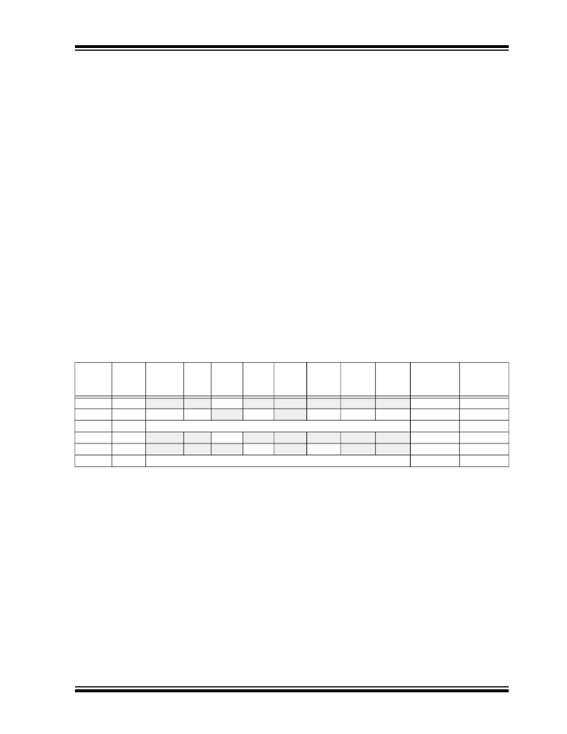
TABLE 12-7:
REGISTERS ASSOCIATED WITH ASYNCHRONOUS RECEPTION
Address
Name
Bit 7
Bit 6
Bit 5
Bit 4
Bit 3
Bit 2
Bit 1
Bit 0
Value on
POR
Value on
all other
RESETS
0Ch
PIR1
EEIF
CMIF
RCIF
TXIF
—
CCP1IF TMR2IF TMR1IF
0000 -000 0000 -000
18h
RCSTA
RCREG USART Receive data registe
r
SPEN
RX9
SREN
CREN
ADEN
FERR
OERR
RX9D
0000 000x 0000 000x
1Ah
0000 0000 0000 0000
8Ch
PIE1
EEIE
CMIE
RCIE
TXIE
—
CCP1IE TMR2IE TMR1IE
0000 -000 0000 -000
98h
TXSTA
CSRC
TX9
TXEN
SYNC
—
BRGH
TRMT
TX9D
0000 -010 0000 -010
99h
SPBRG Baud Rate Generator Register
0000 0000 0000 0000
Legend:
x
= unknown,
-
= unimplemented locations read as '0'. Shaded cells are not used for Asynchronous Reception.
相關(guān)PDF資料 |
PDF描述 |
|---|---|
| 16M0 | PC SERIAL MODEM CBL 50 FT |
| 16M0B | APPLE IIC CABLE TO IWRTR MODEM |
| 16M0BC | KEYBD.EXT. MINI DIN 4 MM 6 FT |
| 16M0BS | KEYBD.EXT. MINI DIN 4 MM 10 FT |
| 16M0D | MINI DIN 8, MALE-MALE 10 FT. |
相關(guān)代理商/技術(shù)參數(shù) |
參數(shù)描述 |
|---|---|
| 16F630 | 制造商:MICROCHIP 制造商全稱:Microchip Technology 功能描述:14-Pin FLASH-Based 8-Bit CMOS Microcontrollers |
| 16F684-I | 制造商:Microchip Technology Inc 功能描述: |
| 16F6H | 制造商:EDAL 制造商全稱:EDAL 功能描述:Silicon High Voltage Assembly |
| 16F6H1 | 制造商:EDAL 制造商全稱:EDAL 功能描述:Silicon High Voltage Assembly |
| 16F7674 | 制造商:未知廠家 制造商全稱:未知廠家 功能描述:SMD TWEEZER HEAD |
發(fā)布緊急采購,3分鐘左右您將得到回復。